Space & Physics
India Semiconductor Mission: ‘It’s Not About Fabs. It’s About Building An Entire Ecosystem’
India Semiconductor Mission is reshaping the country’s chip ambitions. Neelkanth Mishra explains the opportunities, challenges and long-term strategy.

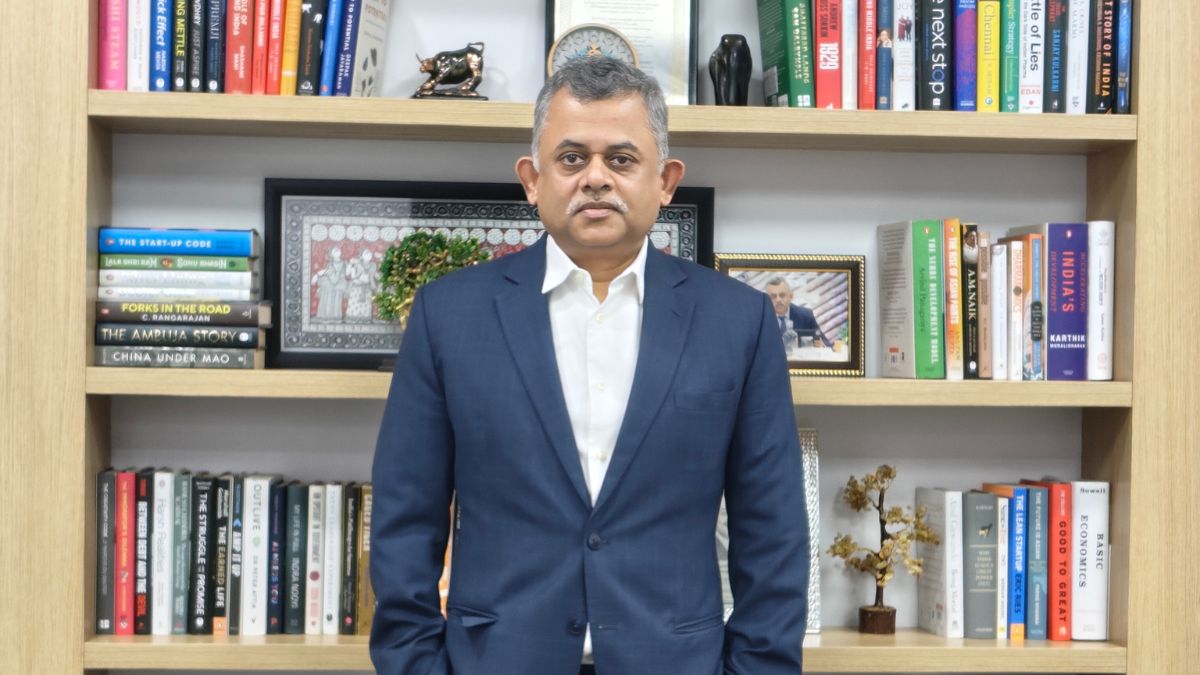
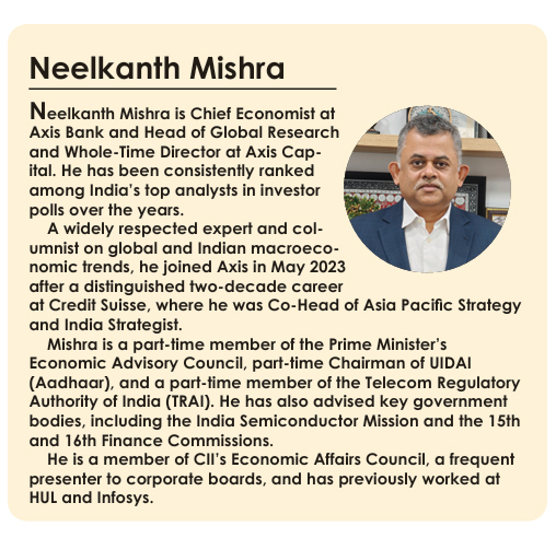
As India pushes ahead with its semiconductor ambitions under the India Semiconductor Mission (ISM), questions remain about where the country can realistically compete and how long it will take to build a viable ecosystem. In this exclusive conversation with Education Publica Editor Dipin Damodharan in Mumbai, Neelkanth Mishra, Chief Economist at Axis Bank and Head of Global Research at Axis Capital, draws on two decades of experience tracking the global semiconductor industry to explain India’s advantages, constraints, and long term trajectory. He is also a member of the advisory committee of the government’s India Semiconductor Mission and part-time Chairperson of the Unique Identification Authority of India (UIDAI). Edited excerpts.
How the India Semiconductor Mission Is Shaping the Industry
Let me start with asking something out of curiosity – how did you get interested in semiconductors in the first place?
When I joined Credit Suisse First Boston in 2003 in Singapore, the person who hired me was heading Asia technology research and was also the lead analyst for semiconductor foundries such as TSMC and UMC. I was hired to cover IT services, but he wanted help in building the semiconductor research franchise.
That led me to start reading about how chips are made. At that time, the industry was transitioning from 130-nanometer to 90-nanometer nodes, and copper was being introduced to replace aluminum due to resistance issues. There were challenges around yields because copper was seeping into substrates. I remember writing my first note around this issue after going through technical papers.

That note became quite popular, and it gave me the confidence to continue covering semiconductors. I spent a lot of time travelling to Taiwan, studying DRAM cycles, capex cycles, node transitions, and the broader global semiconductor ecosystem. Eventually, I moved to Taipei and began covering chip design companies such as MediaTek.
At that time, were you also tracking what was happening in India?
India has had chip design activity for a long time, even in the 1990s. Companies like Texas Instruments, Cadence, and Synopsys were recruiting from Indian campuses. Many engineers built long careers in these firms.
However, India did not have domestic chip manufacturing or strong Indian-owned chip design companies. By the mid-2000s, global firms such as Nvidia, Broadcom, and Intel began setting up design centres in India. So the design ecosystem was growing, but it was largely driven by global companies.
It is only in the last four to five years that more serious efforts have begun toward building Indian-owned capabilities.
So what changed in the last few years? Was it policy, or something else?
Policy has played a role. The Design Linked Incentive (DLI) scheme has been an important catalyst. We are seeing some early success. At the same time, there is also an evolutionary factor at play. Engineers who moved abroad 20–25 years ago are now at a stage where they have both the experience and financial capacity to take entrepreneurial risks. Many also want to return to India.
Another important factor is the growth of India’s electronics manufacturing ecosystem. As assembly volumes increase, there is greater awareness of what products need to be designed. Without that visibility into OEM pipelines, it is difficult to design chips.
Schemes like PLI for electronics manufacturing have helped build that awareness and ecosystem. As downstream industries grow, upstream opportunities in chip design also become clearer.
As US is good at designing chips, Taiwan and South Korea are good at manufacturing There’s always this question – should India focus on design, manufacturing, or packaging?
There is no either/or. India needs to participate across the value chain.
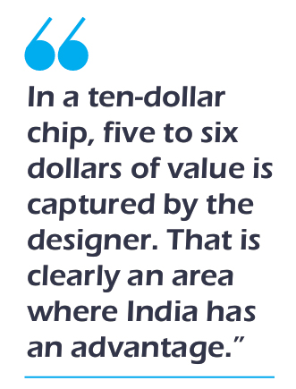
We already have a natural advantage in chip design, with about 20% of global design engineers based in India. Design is also less capital-intensive compared to manufacturing. In a $10 chip, $5–6 of value is captured by the designer, and in some cases even more.
At the same time, semiconductor manufacturing is a geopolitical necessity. It is not just a commercial issue but also a matter of national security. That is why governments provide significant subsidies for fabs.
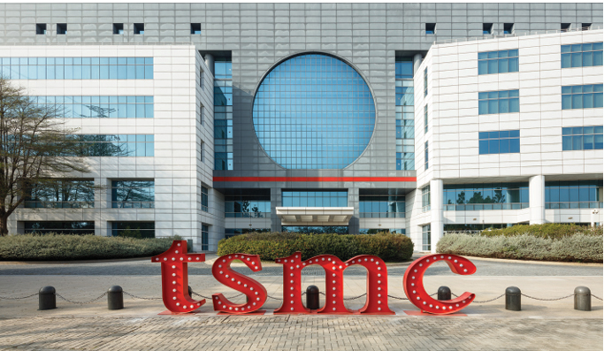
However, manufacturing is a low-return business globally. Only a few companies like TSMC and Samsung have consistently generated returns above their cost of capital. Much of the value in the ecosystem is captured by design firms and by capital equipment suppliers, which operate in highly concentrated markets.
Therefore, India must build capabilities across the chain—from design to manufacturing to equipment and materials—if it wants meaningful value capture.
When we talk about building an ecosystem, how complex is that in reality?
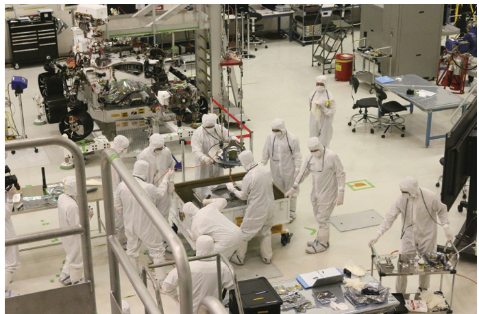
It is extremely complex. The industry has multiple layers of specialization. For example, electronic design automation (EDA) tools are dominated by a few companies. Lithography, especially extreme ultraviolet, is controlled by a single company globally. Equipment for deposition, wafer slicing, and testing is also concentrated among a handful of firms.
Even the chemicals used in wafer cleaning are highly sophisticated and require extraordinary purity. A single wafer can take months to manufacture, involving hundreds of process steps.
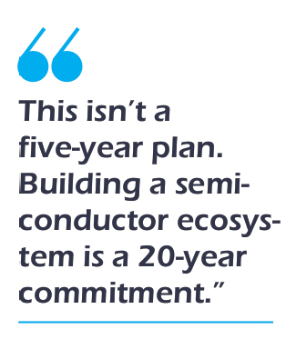
So when we talk about semiconductors, it is not just about fabs. It is about building an entire ecosystem—equipment, materials, design, testing, and packaging. This is why it is a 15–20 year journey at least.
What about talent? Are we ready from a skills perspective?
In general, skilling in India is more of a demand problem than a supply problem. If there is sufficient demand, the industry tends to create the supply.
For example, there is already discussion about developing tens of thousands of chip testing engineers in India, and that is achievable. However, for cutting-edge technologies, there is a need for deeper investment in research.
As we move toward more advanced nodes—such as 7 to 12 nanometers—we will require significant high-end research capabilities. Countries like China took over 25 years to reach that level.
We need to invest not just in near-commercial research (TRL 6–9) but also in fundamental research (TRL 1–4), which creates long-term intellectual property. Government initiatives like the Anusandhan National Research Fund are steps in that direction, but overall R&D spending needs to increase.
What role should industry play in R&D?
Industry participation is essential. The government can catalyse investment, but companies will invest when they see potential returns.
We have seen this in pharmaceuticals, where Indian firms moved into R&D after reaching limits in generics. A similar shift can happen in semiconductors, but it will require scale, capital, and long-term commitment.
Where do startups fit into this picture?
Startups will have a significant role, particularly in chip design. Manufacturing is extremely capital-intensive, requiring billions of dollars in investment, which limits the role of startups.
However, in design and innovation, startups can play an important part. Many innovations in the semiconductor ecosystem originate from smaller firms, which are later acquired or integrated into larger companies.
To produce a globally competitive company, you need a large ecosystem of startups, experimentation, and risk-taking.
Coming to policy – what did India learn from ISM 1.0?
ISM 1.0 (India Semiconductor Mission) was a learning curve for everyone. It helped the government understand how to evaluate proposals, support companies, and manage operational challenges.
There were practical issues—from customs procedures affecting sensitive equipment to ensuring uninterrupted power supply. Semiconductor manufacturing requires extremely high reliability, and even a brief power outage can cause significant losses.
Another important learning is that the global industry is now more comfortable working with India. While India may not yet be the first choice, confidence has improved due to visible commitment and progress.
This increased comfort allows India to be more ambitious with ISM 2.0.
How important is policy stability?
Policy continuity is very important because these are long-term projects. Global firms value consistency in decision-making and relationships.
There is also a growing effort to ensure continuity in leadership within government institutions, which helps build expertise and trust over time.
Do we need a dedicated semiconductor research institution like IMEC?
There are existing efforts, such as the facility in Mohali, which supports defence-related applications. There are also discussions around creating IMEC-like research centres.
However, over time, the private sector will need to take a larger role in research. Government support is critical in the early stages, but for sustained innovation and competitiveness, industry-led initiatives are more effective. The government can act as the binding force or the catalyst that brings people to the table; however, I believe it is ultimately better if the private sector takes the lead. This creates a natural incentive for innovation and rigorous research. Beyond a certain point, government support becomes both fiscally unfeasible and operationally undesirable
If we look ahead 20 years, where do you see India?
On the design side, India can become much more significant. It is possible to see 10–15 large chip design companies and many smaller firms emerging.
On the manufacturing side, we could have several large fabs and potentially global players establishing operations in India, especially if a strong domestic design ecosystem develops.
For example, companies like TSMC tend to follow innovation ecosystems. If Indian design firms grow in scale and sophistication, it could attract global manufacturing investments.
Let me end with this – can India produce a company like Nvidia?
It is possible, but it requires a large ecosystem. Many Indians already occupy senior roles in global semiconductor companies and are involved in cutting-edge design work.
To create a company of that scale, you need risk capital, entrepreneurial ambition, and a large number of startups. In other markets, hundreds of firms compete, and one eventually emerges as a dominant player.
So it is not about a single effort—it is about building an ecosystem where many experiments take place, and success emerges from that.




Space & Physics
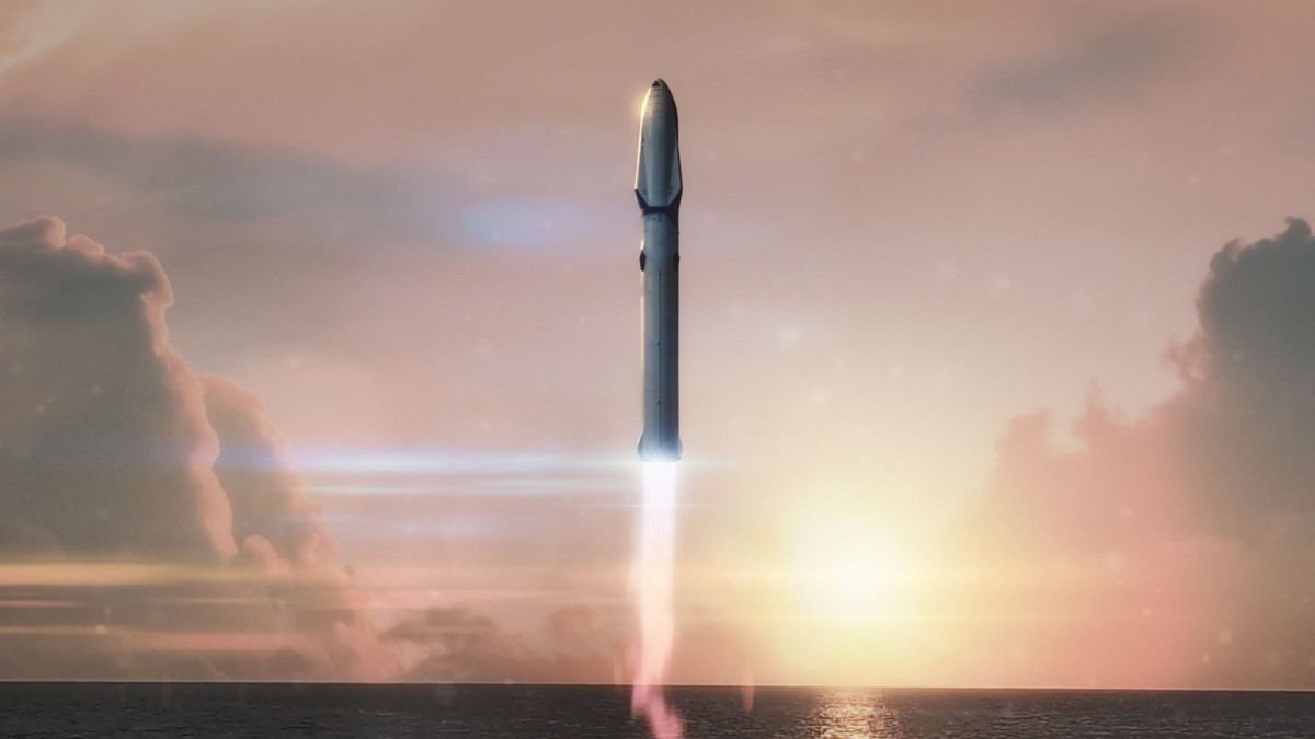
World Space Week 2026: How the Rocket Revolution Is Changing Space
World Space Week 2026 explores the Rocket Revolution, from reusable launchers and private space companies to the growing role of satellites.

Space & Physics
A Dead Star Feeds Off Planet Formed From Its Ashes
It adds to a known coterie of planets now found orbiting dead stars, astronomers are busy studying to spot signs of life.

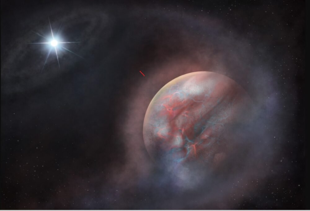
A planet orbiting once every 4 days around a white dwarf star HS 0209+0832 – about 270 light years in the direction of the constellation Pisces – is steadily losing its atmosphere to its host star. While many stars in solar systems beyond our own often feed on their planets, this particular star feeds on its own ashes.
The gaseous planet HS 0209+0832 b was discovered in 2024, when the Transiting Exoplanet Survey Satellite, a NASA space telescope, found it orbiting the white dwarf star over the course of four days. The new study followed through with detailed observations from TESS data, NASA’s space-based Far Ultraviolet Spectroscopic Explorer, in addition to the ESO’s mountain-based Very Large Telescope, to study the star’s atmosphere and in turn inferring some chemistry occurring in the planet.
In a study published in the journal Nature Astronomy on Monday and funded by NASA, European Research Council, Fundación Occident and the Instituto de Astrofísica de Canarias, an international team of astronomers have reported imprints of niobium, a heavy element, in the atmosphere of a white dwarf star.
Astronomers predict the transiting young planet around the dead star is supplying that niobium back to its host. The sighting is evidence of a “second generation” planet, one of many candidates identified over several years, manifesting in a myriad different ways from spent gas ejected in the wake of stellar deaths.
It adds to a known coterie of planets now found orbiting dead stars, astronomers are busy studying to spot signs of life.
What are white dwarf stars?
White dwarves are an exotic stars, and are all that’s left off giant stars shedding their large gaseous skin in violent deaths. Our sun is destined one day to transform into a white dwarf, but only after swelling in size some five billion years from now to become a red giant when it will eclipse past the earth’s orbit. It would take several million years after that for the red giant sun to shed its gaseous exterior to become a white dwarf.
Planets if any, found orbiting these dead stars may have likely migrated from the new solar system’s outer reaches. All that’s left off the progenitor star’s past are imprints of light metals and other elements on the white dwarf’s atmosphere. Such planets have previously been spotted orbiting pulsars, a kind of neutron star, back in 1992. In fact, its discovery had marked the first ever detection of any planet orbiting a star beyond our sun.

In five billion years, our sun will evolve to become a red giant star. Credit: Svitlana Leonidivna Malchenko
Sighting niobium
Elements such as niobium don’t typically form in the core of stars like our sun. Chemical production usually limits to elements lighter than or until iron, with its 26 protons and 30 neutrons. Beyond that, slamming an extra proton or neutron will cause those to split, leaving iron to be the last element to be directly forged.
Niobium, with 41 protons and 52 neutrons, is thought to be born after absorbing slow passing neutrons when the red giant star dies to form a white dwarf star. This niobium hitches a ride along with rest of the contents of the red giant star, farther into the outer reaches of the system after the formation of the white dwarf.
These contents could create a new disc of circumstellar material with dust and gas that could condense one day to form new planets. The “second generation” planet found orbiting the white dwarf star from the new study, could have been born this way.
Alternatively, it may have been a planet in the outskirts like Neptune, migrating inwards, and enriching itself with niobium-rich star material.
Either way, the planet got too close to its host star, which is irradiating its newfound niobium-rich atmosphere, stripping it away and devouring it.
While it’s likely not a candidate planet for life as we know it to be found, it’s discovery can help ascertain how such worlds are formed in the aftermath of a star’s various phases of evolution.
Space & Physics
Artemis Accords Reach 76 Countries: What It Means for India
The Artemis Accords now have 76 signatories. With NASA inviting ISRO to its Moon Base programme, India’s role in lunar exploration is expanding.
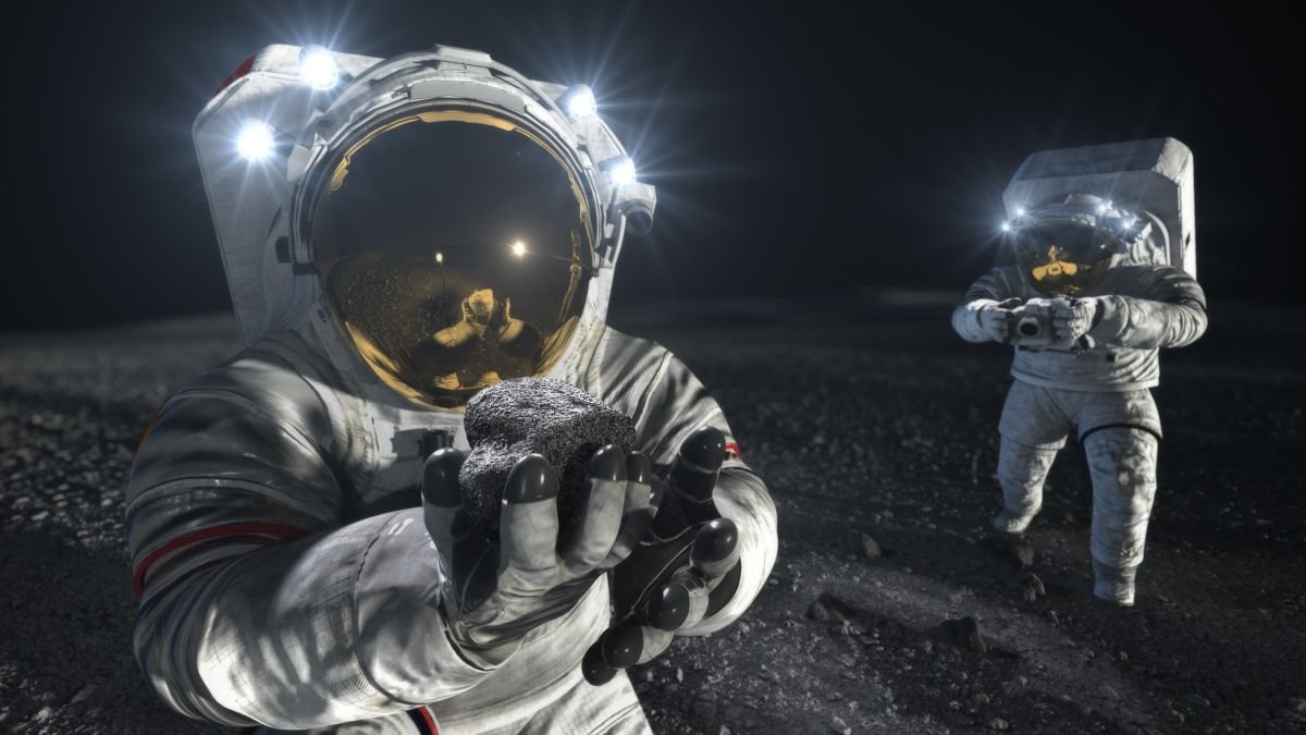
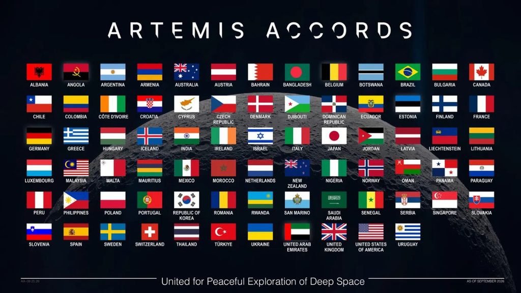
The Artemis Accords now have 76 signatories, expanding the international framework around the next phase of lunar exploration. For India, the milestone comes weeks after NASA invited the Indian Space Research Organisation (ISRO) to participate in its planned Moon Base programme.
Albania, Croatia, Côte d’Ivoire and San Marino joined the Accords in September, taking participation to 76 countries. NASA says nearly 40% of the world’s nations are now part of the framework, which sets principles for peaceful, transparent and responsible exploration of the Moon, Mars and beyond.
India became the 27th signatory in June 2023. At the India-US Civil Space Joint Working Group meeting in Bengaluru in August, NASA invited ISRO to participate in its Moon Base programme. The two countries also agreed to advance discussions on open scientific-data sharing under the Accords.
India’s Moon Base opportunity
The invitation does not specify what India will contribute. NASA has said every Artemis Accords signatory can participate through scientific payloads, technology demonstrations, CubeSats and other capabilities. Any specific Indian contribution would require further agreements.
India, however, is developing its own increasingly ambitious lunar programme. ISRO’s Chandrayaan-4 is planned as a lunar sample-return mission, designed to collect samples from the Moon’s polar region and bring them back to Earth. Chandrayaan-5/LUPEX, being developed with Japan’s JAXA, will study lunar polar volatiles in situ.
These missions could give India experience and scientific capabilities relevant to a future international lunar infrastructure.
ISRO Shaping the Data Conversation
Scientific data could be another area of Indian participation. In May 2026, ISRO led an initial Artemis Accords discussion on advancing open-data practices. NASA subsequently held two workshops focused on making lunar scientific data more accessible, interoperable and reproducible across countries.
That is significant as more lunar missions target the same regions. Shared standards could allow researchers to combine observations from different spacecraft instead of treating each mission’s data separately.
Moon – Space Coperation
India-US space cooperation is also expanding into human spaceflight. ISRO’s 2025–26 annual report records that Indian astronaut Shubhanshu Shukla travelled to the International Space Station in June 2025 as part of the Axiom-4 mission and conducted seven microgravity experiments. ISRO also held discussions with NASA on potential cooperation related to Gaganyaan.
The Artemis relationship therefore sits alongside an existing programme of India-US cooperation, including the NASA-ISRO Synthetic Aperture Radar (NISAR) mission.
What Changes for India?
The significance of the 76-country milestone lies in the network developing around it. The Artemis Accords cover scientific-data sharing, interoperability, non-interference between missions, emergency assistance and protection of historically significant lunar sites. NASA says signatories are now working through technical meetings and workshops to put these principles into practice.
For India, that creates several possible avenues: contributing technology or science to NASA’s Moon Base effort, sharing lunar data, and working with a growing group of countries on standards for increasingly crowded lunar operations. What India’s specific contribution to the Moon Base remains undecided. But with Chandrayaan-4, LUPEX and its human-spaceflight programme advancing alongside deeper NASA cooperation, India is entering the next phase of lunar exploration with its own capabilities already taking shape.


Global Job Market Faces a Growing Inclusion Gap as AI and Digitalisation Reshape Work

FSSAI Moves to Restrict Added Sugars in Infant Foods, Citing Need for Stronger Nutritional Safeguards

NMC Directs Medical Colleges to Set Up Patient Safety Committees

The Monsoon’s New Rhythm: Less Rain, More Intense Downpours

World Food Day: India’s Childhood Obesity Burden Raises Concerns Over Diabetes Risk

From Scams to Screens: How the National Stock Exchange Rewrote India’s Equity Story

Knowing When to Think for Ourselves: AI, Intuition and the Education of Discernment

After a Scorching Summer, Delhi’s Children Are Slow to Return Outdoors

Two Chemists Win Nobel Prize for Solving a Century-Old Puzzle: Why Life Picks One Hand Over the Other

India’s AI Moment Rests on More Than Code

-

 Math3 months ago
The 2026 Fields Medals: Four Proofs, Four Decades-Old Problems Solved
-
EP Deep Dive: Data & Solutions3 months ago
After Kerala’s Deadliest Landslide, the Hardest Thing to Rebuild Was Childhood
-
EP Deep Dive: Data & Solutions3 months ago
West Asia Crisis: Can Kerala’s Returning Gulf Migrants Find a Future in the Green Economy?
-
Interviews4 weeks ago
From Scams to Screens: How the National Stock Exchange Rewrote India’s Equity Story
-
Climate5 months ago
The Climate World Cup? How Climate Change Could Affect Player Performance at the 2026 World Cup
-
Society3 months ago
What Is Civilisational Diplomacy? Understanding India’s Newest Foreign Policy Tool
-
Society4 months ago
From Bell Labs to the Classroom: A Second Career in Teaching
-
Space & Physics5 months ago
Engineers Develop Dual-Mode Propulsion System for Next-Generation Small Satellites