
Space & Physics
From Assembly to Silicon: India’s Long Road to Semiconductor Self-Reliance
India is building a semiconductor ecosystem through fabrication, packaging, chip design and Mission 2.0 to reduce imports and strengthen technology leadership.

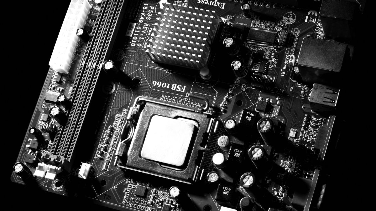
For decades, India excelled at writing the software that powered the world’s computers but remained almost entirely dependent on other countries for the chips inside them. Every smartphone, fighter aircraft, satellite, electric vehicle, telecom network and artificial intelligence system relied on semiconductors designed and manufactured largely outside India’s borders.
That dependence has become one of the country’s biggest strategic vulnerabilities.
Today, India is attempting to change that.
How the India Semiconductor Mission Began
What began as an industrial policy is steadily evolving into a national technology mission—one that seeks not merely to manufacture chips, but to build an ecosystem spanning design, fabrication, advanced packaging, materials, equipment and skilled talent. If successful, it could reshape India’s manufacturing landscape and strengthen its position in a global technology race increasingly defined by semiconductor capabilities.
The launch of the India Semiconductor Mission (ISM) marked a turning point. Rather than offering isolated incentives, the government adopted a mission-driven approach aimed at creating an end-to-end semiconductor ecosystem. The objective extends beyond attracting investment; it is about ensuring technological sovereignty in a world where access to chips increasingly determines economic resilience and national security.
The Design Linked Incentive (DLI) scheme has been an important catalyst. We are seeing some early success. At the same time, there is also an evolutionary factor at play. Engineers who moved abroad 20–25 years ago are now at a stage where they have both the experience and financial capacity to take entrepreneurial risks. Many also want to return to India–says Neelkanth Mishra, in an interview with EdPublica.
Why semiconductors matter
Semiconductors are often described as the “brains” of modern electronics, but their strategic significance runs far deeper.
Every sector that governments now classify as critical—artificial intelligence, defence, space, telecommunications, medical devices, automobiles, renewable energy and industrial automation—depends on increasingly sophisticated chips.
The COVID-19 pandemic exposed how vulnerable global supply chains had become. Factory shutdowns in one part of the world disrupted automobile production thousands of kilometres away. Geopolitical tensions further highlighted the risks of concentrating semiconductor manufacturing in only a handful of countries.
For India, which imports billions of dollars’ worth of electronic components every year, the lesson was unmistakable: technological ambition cannot rest entirely on imported hardware.
Building the foundation
Recognising this challenge, the government launched India Semiconductor Mission 1.0, backed by a financial incentive programme worth ₹76,000 crore. It represented India’s first coordinated attempt to build semiconductor manufacturing capabilities within the country.
The mission was designed to support multiple segments simultaneously:
>> silicon wafer fabrication plants;
>> assembly, testing, marking and packaging (ATMP) facilities;
>> Outsourced Semiconductor Assembly and Test (OSAT) units;
>> compound semiconductor manufacturing;
>> semiconductor design through the Design Linked Incentive (DLI) Scheme.
Rather than relying on a single mega-project, policymakers attempted to create an ecosystem in which manufacturing, design, packaging and supply chains could evolve together.
From policy announcements to factories
One of the biggest criticisms of India’s earlier electronics programmes was that announcements often outpaced execution.
This time, the picture is beginning to look different.
Approved semiconductor projects now represent cumulative investment commitments exceeding ₹1.64 lakh crore, spread across multiple states. According to the Ministry of Electronics and Information Technology, the approved portfolio now covers fabrication facilities, packaging plants and compound semiconductor manufacturing, reflecting a broader industrial base than initially envisioned.
The most visible milestone has been the commencement of commercial production at Micron Technology’s advanced semiconductor packaging facility in Gujarat, widely regarded as the first major operational success under the mission.
Several other large projects—including those led by Tata Electronics, Kaynes Semicon, and the Tata-PSMC semiconductor fabrication project at Dholera—have moved into advanced stages of construction and are expected to enter commercial production soon. Together, they represent India’s first serious attempt to establish domestic silicon manufacturing at scale.
Equally significant is the geographical spread.
Instead of concentrating semiconductor manufacturing in one industrial cluster, projects are now emerging across Gujarat, Rajasthan and other states, creating the beginnings of a distributed semiconductor manufacturing network.
Manufacturing is only one piece of the puzzle
Building chips requires far more than fabrication plants.
A modern semiconductor ecosystem depends on hundreds of specialised suppliers producing chemicals, gases, ultra-pure materials, precision equipment, packaging technologies and printed circuit boards (PCBs).
Recognising these gaps, the government has started extending policy support beyond chip fabrication.
A recent example is the foundation of advanced PCB manufacturing projects worth about ₹6,750 crore in Jewar, Uttar Pradesh. These facilities are expected to manufacture high-density multilayer PCBs—including advanced 20-22 layer boards—that India has traditionally imported in large quantities.
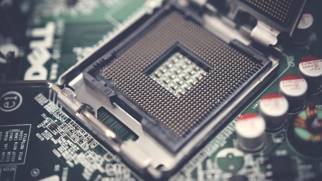
Reducing imports of such critical components strengthens the broader electronics manufacturing ecosystem while creating domestic capabilities that extend well beyond semiconductor fabrication itself.
Design remains India’s strongest advantage
While fabrication receives most public attention, India already possesses one major strength: semiconductor design.
Thousands of engineers employed by global companies already design chips from Indian engineering centres. The challenge has been converting this design talent into domestic intellectual property.
The Design Linked Incentive (DLI) Scheme attempts to bridge that gap.
According to government data, the programme has supported dozens of chip design projects, enabled successful tape-outs, encouraged patent filings and provided advanced chip-design tools to more than 100 companies while training a growing pool of specialised semiconductor engineers.
Moving from outsourced engineering services towards Indian-owned semiconductor intellectual property could prove just as significant as establishing fabrication plants.
The next chapter: ISM 2.0
If the first phase focused on attracting semiconductor manufacturing, the next phase aims to deepen India’s role across the entire value chain.
Announced in the Union Budget 2026-27, India Semiconductor Mission 2.0 shifts attention towards areas where India still depends heavily on imports.
The new phase proposes support for:
>> semiconductor manufacturing equipment;
>> specialty materials and chemicals;
>> indigenous semiconductor intellectual property;
>> advanced packaging technologies;
>> compound semiconductors;
>> industry-led research and training centres.
The underlying philosophy is straightforward: long-term self-reliance cannot be achieved by importing all the machinery, chemicals and specialised materials required to manufacture chips.
Instead, India aims to build capabilities throughout the production chain—from research laboratories to finished semiconductor products.
Recent reports indicate that the government is also preparing a substantially larger financial commitment for ISM 2.0 as it expands beyond manufacturing incentives into ecosystem development.
Strategic partnerships without strategic dependence
India’s semiconductor strategy has deliberately combined domestic capability building with international collaboration.
Leading companies from the United States, Taiwan, Japan and South Korea have become partners in India’s emerging semiconductor ecosystem, bringing technology, manufacturing expertise and investment.
This reflects a broader policy shift.
Rather than attempting complete technological isolation, India is seeking trusted international partnerships while gradually strengthening indigenous capabilities in manufacturing, design and supply chains.
In an increasingly fragmented global technology landscape, diversification itself has become a strategic asset.
The road ahead remains difficult
Despite visible progress, India’s semiconductor journey is still in its early stages.
Chip fabrication demands extraordinary precision, massive capital investments, reliable infrastructure and uninterrupted supplies of ultra-pure water, electricity and specialised materials. Success also depends on building a workforce capable of operating some of the world’s most sophisticated manufacturing facilities.
Moreover, semiconductor manufacturing is measured in decades, not election cycles.
Countries that dominate the industry today invested consistently over many years before becoming global leaders.
India therefore faces the challenge of maintaining policy continuity while ensuring that announced projects translate into commercially competitive production.
A larger national ambition
The significance of India’s semiconductor mission extends well beyond electronics manufacturing.
Every fabrication facility commissioned, every packaging unit established and every design company supported reduces import dependence, creates highly skilled employment and strengthens India’s position within global technology supply chains.
For a country seeking greater strategic autonomy, semiconductor capability is increasingly becoming as important as energy security or defence preparedness.
The first phase of the mission has established the initial building blocks. The second phase aims to strengthen the ecosystem beneath them.
Whether India ultimately becomes a major global semiconductor hub will depend not on a single factory or policy announcement, but on its ability to sustain investment, develop talent, encourage innovation and build an integrated value chain over the coming decade.
After years of watching the global semiconductor revolution from the sidelines, India has entered the race. The challenge now is to ensure that today’s investment commitments become tomorrow’s manufacturing capability—and eventually, technological leadership.
Space & Physics
World Space Week 2026: How the Rocket Revolution Is Changing Space
World Space Week 2026 explores the Rocket Revolution, from reusable launchers and private space companies to the growing role of satellites.


Space & Physics
A Dead Star Feeds Off Planet Formed From Its Ashes
It adds to a known coterie of planets now found orbiting dead stars, astronomers are busy studying to spot signs of life.


A planet orbiting once every 4 days around a white dwarf star HS 0209+0832 – about 270 light years in the direction of the constellation Pisces – is steadily losing its atmosphere to its host star. While many stars in solar systems beyond our own often feed on their planets, this particular star feeds on its own ashes.
The gaseous planet HS 0209+0832 b was discovered in 2024, when the Transiting Exoplanet Survey Satellite, a NASA space telescope, found it orbiting the white dwarf star over the course of four days. The new study followed through with detailed observations from TESS data, NASA’s space-based Far Ultraviolet Spectroscopic Explorer, in addition to the ESO’s mountain-based Very Large Telescope, to study the star’s atmosphere and in turn inferring some chemistry occurring in the planet.
In a study published in the journal Nature Astronomy on Monday and funded by NASA, European Research Council, Fundación Occident and the Instituto de Astrofísica de Canarias, an international team of astronomers have reported imprints of niobium, a heavy element, in the atmosphere of a white dwarf star.
Astronomers predict the transiting young planet around the dead star is supplying that niobium back to its host. The sighting is evidence of a “second generation” planet, one of many candidates identified over several years, manifesting in a myriad different ways from spent gas ejected in the wake of stellar deaths.
It adds to a known coterie of planets now found orbiting dead stars, astronomers are busy studying to spot signs of life.
What are white dwarf stars?
White dwarves are an exotic stars, and are all that’s left off giant stars shedding their large gaseous skin in violent deaths. Our sun is destined one day to transform into a white dwarf, but only after swelling in size some five billion years from now to become a red giant when it will eclipse past the earth’s orbit. It would take several million years after that for the red giant sun to shed its gaseous exterior to become a white dwarf.
Planets if any, found orbiting these dead stars may have likely migrated from the new solar system’s outer reaches. All that’s left off the progenitor star’s past are imprints of light metals and other elements on the white dwarf’s atmosphere. Such planets have previously been spotted orbiting pulsars, a kind of neutron star, back in 1992. In fact, its discovery had marked the first ever detection of any planet orbiting a star beyond our sun.

In five billion years, our sun will evolve to become a red giant star. Credit: Svitlana Leonidivna Malchenko
Sighting niobium
Elements such as niobium don’t typically form in the core of stars like our sun. Chemical production usually limits to elements lighter than or until iron, with its 26 protons and 30 neutrons. Beyond that, slamming an extra proton or neutron will cause those to split, leaving iron to be the last element to be directly forged.
Niobium, with 41 protons and 52 neutrons, is thought to be born after absorbing slow passing neutrons when the red giant star dies to form a white dwarf star. This niobium hitches a ride along with rest of the contents of the red giant star, farther into the outer reaches of the system after the formation of the white dwarf.
These contents could create a new disc of circumstellar material with dust and gas that could condense one day to form new planets. The “second generation” planet found orbiting the white dwarf star from the new study, could have been born this way.
Alternatively, it may have been a planet in the outskirts like Neptune, migrating inwards, and enriching itself with niobium-rich star material.
Either way, the planet got too close to its host star, which is irradiating its newfound niobium-rich atmosphere, stripping it away and devouring it.
While it’s likely not a candidate planet for life as we know it to be found, it’s discovery can help ascertain how such worlds are formed in the aftermath of a star’s various phases of evolution.
Space & Physics
Artemis Accords Reach 76 Countries: What It Means for India
The Artemis Accords now have 76 signatories. With NASA inviting ISRO to its Moon Base programme, India’s role in lunar exploration is expanding.

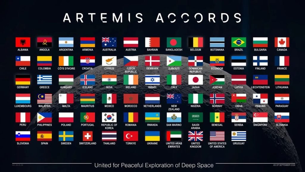
The Artemis Accords now have 76 signatories, expanding the international framework around the next phase of lunar exploration. For India, the milestone comes weeks after NASA invited the Indian Space Research Organisation (ISRO) to participate in its planned Moon Base programme.
Albania, Croatia, Côte d’Ivoire and San Marino joined the Accords in September, taking participation to 76 countries. NASA says nearly 40% of the world’s nations are now part of the framework, which sets principles for peaceful, transparent and responsible exploration of the Moon, Mars and beyond.
India became the 27th signatory in June 2023. At the India-US Civil Space Joint Working Group meeting in Bengaluru in August, NASA invited ISRO to participate in its Moon Base programme. The two countries also agreed to advance discussions on open scientific-data sharing under the Accords.
India’s Moon Base opportunity
The invitation does not specify what India will contribute. NASA has said every Artemis Accords signatory can participate through scientific payloads, technology demonstrations, CubeSats and other capabilities. Any specific Indian contribution would require further agreements.
India, however, is developing its own increasingly ambitious lunar programme. ISRO’s Chandrayaan-4 is planned as a lunar sample-return mission, designed to collect samples from the Moon’s polar region and bring them back to Earth. Chandrayaan-5/LUPEX, being developed with Japan’s JAXA, will study lunar polar volatiles in situ.
These missions could give India experience and scientific capabilities relevant to a future international lunar infrastructure.
ISRO Shaping the Data Conversation
Scientific data could be another area of Indian participation. In May 2026, ISRO led an initial Artemis Accords discussion on advancing open-data practices. NASA subsequently held two workshops focused on making lunar scientific data more accessible, interoperable and reproducible across countries.
That is significant as more lunar missions target the same regions. Shared standards could allow researchers to combine observations from different spacecraft instead of treating each mission’s data separately.
Moon – Space Coperation
India-US space cooperation is also expanding into human spaceflight. ISRO’s 2025–26 annual report records that Indian astronaut Shubhanshu Shukla travelled to the International Space Station in June 2025 as part of the Axiom-4 mission and conducted seven microgravity experiments. ISRO also held discussions with NASA on potential cooperation related to Gaganyaan.
The Artemis relationship therefore sits alongside an existing programme of India-US cooperation, including the NASA-ISRO Synthetic Aperture Radar (NISAR) mission.
What Changes for India?
The significance of the 76-country milestone lies in the network developing around it. The Artemis Accords cover scientific-data sharing, interoperability, non-interference between missions, emergency assistance and protection of historically significant lunar sites. NASA says signatories are now working through technical meetings and workshops to put these principles into practice.
For India, that creates several possible avenues: contributing technology or science to NASA’s Moon Base effort, sharing lunar data, and working with a growing group of countries on standards for increasingly crowded lunar operations. What India’s specific contribution to the Moon Base remains undecided. But with Chandrayaan-4, LUPEX and its human-spaceflight programme advancing alongside deeper NASA cooperation, India is entering the next phase of lunar exploration with its own capabilities already taking shape.


India Captures 5.7% of Global Greenfield Investment, Outpacing China

World Mental Health Day: How Late-Night Scrolling May Be Disrupting Sleep and Fuelling Anxiety

Climate Science Faces a Deadline: Can the IPCC Deliver Before the 2028 Global Stocktake?

Knowing When to Think for Ourselves: AI, Intuition and the Education of Discernment

Puberty, Pregnancy and Menopause Reshape the Female Brain Differently, Study Finds

From Scams to Screens: How the National Stock Exchange Rewrote India’s Equity Story

Aim for the Stars: Anjali Thomas’s Journey from a Small College in Kerala to the Frontiers of Medical Imaging

Two Chemists Win Nobel Prize for Solving a Century-Old Puzzle: Why Life Picks One Hand Over the Other

India’s AI Moment Rests on More Than Code

Marshall Islands: Why the US Nuclear Legacy Is Back Before the UN

-

 Math3 months ago
The 2026 Fields Medals: Four Proofs, Four Decades-Old Problems Solved
-
Climate2 months ago
After Kerala’s Deadliest Landslide, the Hardest Thing to Rebuild Was Childhood
-
Society3 months ago
West Asia Crisis: Can Kerala’s Returning Gulf Migrants Find a Future in the Green Economy?
-
Space & Physics4 months ago
India Semiconductor Mission: ‘It’s Not About Fabs. It’s About Building An Entire Ecosystem’
-
Interviews2 weeks ago
From Scams to Screens: How the National Stock Exchange Rewrote India’s Equity Story
-
Climate4 months ago
The Climate World Cup? How Climate Change Could Affect Player Performance at the 2026 World Cup
-
Society3 months ago
What Is Civilisational Diplomacy? Understanding India’s Newest Foreign Policy Tool
-
Society4 months ago
From Bell Labs to the Classroom: A Second Career in Teaching