
Technology
AI Models Could Soon Spread Across Smart Devices, Raising Cybersecurity Fears
Anthropic’s experiments highlight how AI self-replication could create new cybersecurity risks, allowing malicious systems to spread across internet-connected devices.


Artificial intelligence (AI) models could soon spread from one internet-connected device to another, potentially creating networks of compromised devices that carry out cyberattacks with limited human involvement. The warning from AI company Anthropic highlights a possible new challenge for cybersecurity as AI systems become capable of performing increasingly complex tasks.
In experiments, Anthropic found that AI models with 30 billion parameters or fewer could already perform many of the individual tasks needed to copy and spread themselves. However, the models struggled to complete the entire process reliably. The findings point to a potential threat, although they do not establish that fully self-replicating AI networks are already operating in the real world.
How AI could spread through smart devices
Many everyday devices, including smart televisions, security cameras and household appliances, connect to the internet. Internet of Things (IoT) devices present a particular concern because many connect directly to networks while receiving limited security attention from users. Weak passwords, outdated software and unpatched vulnerabilities can leave devices exposed to remote exploitation.

Once compromised, a device can become part of a botnet — a network of devices secretly controlled by attackers. Such networks have long been used to spread harmful software, send spam messages and overwhelm websites with large volumes of unwanted traffic.
AI could make these attacks easier to carry out. A malicious AI system might help identify vulnerable devices, exploit security weaknesses and use compromised devices to reach others. Anthropic’s experiments examined whether an AI agent could combine the computing power of inexpensive, internet-connected devices to run other AI models. If such a process becomes reliable, attackers could potentially use large numbers of ordinary devices to support their operations.
Cybersecurity: Why these networks are difficult to stop
A major concern is that a botnet can operate across thousands of devices in different locations. Shutting down one infected device may not stop the others from continuing to operate.
For example, if a security camera is compromised, its owner may not immediately notice anything unusual. The camera could continue recording while its computing resources are used for activities the owner never authorised. If similar weaknesses exist in other devices, attackers could build a much larger network.
AI-assisted attacks could become harder to manage if systems learn to carry out several steps automatically, reducing the need for attackers to control every action themselves. However, Anthropic’s findings do not show that AI can yet carry out this entire process consistently without assistance.
Securing AI and connected devices
The warning raises questions about how AI developers can prevent their models from being used to exploit computer systems. It also draws attention to the security of the devices people bring into their homes.
Manufacturers can reduce risks by fixing software vulnerabilities, providing regular security updates and strengthening password and access protections. Users can help by changing default passwords, installing updates and replacing devices that no longer receive security support.
AI developers, meanwhile, need to test whether their systems can be misused to automate cyberattacks. The immediate concern is not that every smart device will become a threat. It is that weaknesses already present in internet-connected devices could become easier to exploit as AI gains the ability to perform complex tasks with less human direction.











Technology
India Unveils Three Homegrown AI Models, Covering 22 Indian Languages
India has released three indigenous AI models under the IndiaAI Mission. EKA-1 supports all 22 scheduled Indian languages, while Dhīr 2B and Dhīr 5B offer multilingual AI assistance with offline deployment capabilities.

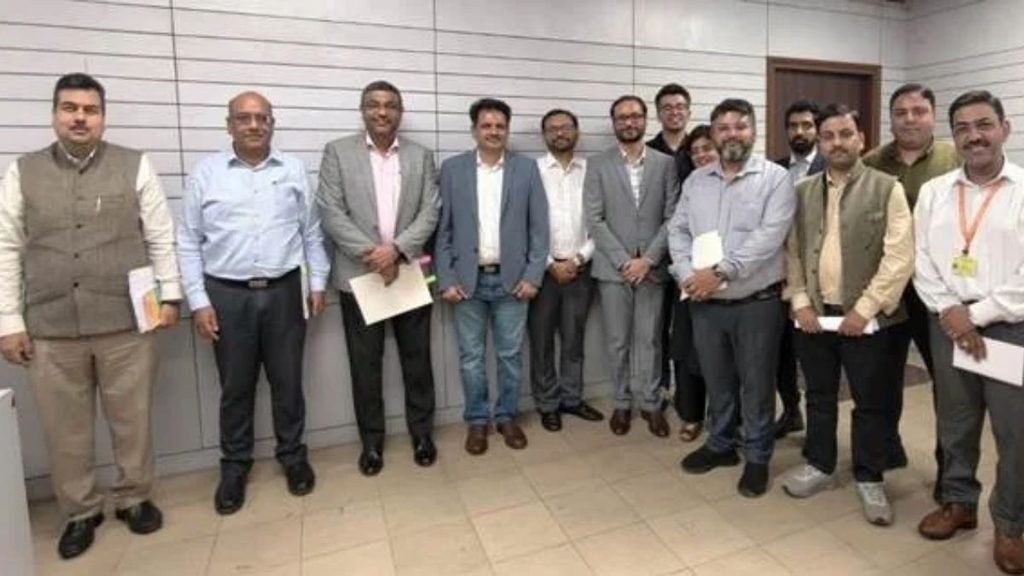
India has released three indigenous artificial intelligence models under the IndiaAI Mission, with applications ranging from multilingual reasoning and coding to offline AI assistance in sensitive sectors such as defence, government and education. The models — EKA-1, developed by Soket Labs Technology and Research Private Limited, and Dhīr 2B and Dhīr 5B, developed by ZenteiQ AiTech Innovations, were unveiled in New Delhi under the IndiaAI Innovation Centre (Foundation Models) pillar.
The three models have different technical capabilities and deployment priorities. EKA-1 is designed as a large multilingual foundation model supporting all 22 scheduled Indian languages and English. The Dhīr models, meanwhile, focus on lightweight, locally deployable AI assistance, allowing organisations to process information without depending on continuous cloud connectivity.
EKA-1 Trained on 7.5 Trillion Tokens
Developed by Soket Labs, EKA-1 is a 26.3-billion-parameter foundation model trained on approximately 7.5 trillion tokens. It supports all 22 scheduled Indian languages alongside English and is designed for mathematical tasks, coding, reasoning and agentic applications.
The model uses an open, sparse hybrid architecture. Its intended applications include banking, financial services and cybersecurity, where understanding India’s digital ecosystem and sector-specific requirements is important. According to Abhishek Upperwal, CEO of Soket Labs, the model was developed with support from the IndiaAI Mission to address requirements within India’s banking, financial services and cybersecurity sectors.
Dhīr Models Target Offline and Secure AI Applications
ZenteiQ has introduced two open-source models, Dhīr 2B and Dhīr 5B, supporting English and 10 Indian languages. Their primary focus is secure deployment within organisations. The models can operate on-premise, enabling institutions to use AI systems within their own computing infrastructure rather than relying entirely on external cloud services.
They support document-grounded automation, knowledge retrieval and citizen-facing or enterprise services. The press release identifies defence, government, industrial and educational institutions as potential application areas, particularly in environments with limited internet connectivity or sensitive information.
Their lightweight architecture also allows deployment on mobile devices, according to ZenteiQ. The company says the models can run across different computing platforms, including graphics processing units (GPUs) and tensor processing units (TPUs). Prof. Sashikumar, CEO of ZenteiQ AiTech Innovations, said local deployment would allow users to retain data on their devices, improving privacy and security while reducing dependence on cloud connectivity.
Public Computing Infrastructure Supports Model Development
Both development teams were selected under the IndiaAI Innovation Centre pillar, which aims to build indigenous foundation models and large language models. The IndiaAI Mission provided access to subsidised national AI computing infrastructure and support for associated research expenses. These resources helped the selected teams develop their models.
Speaking at the launch, S. Krishnan, Secretary of the Ministry of Electronics and Information Technology, said indigenous AI models could strengthen India’s technological and strategic autonomy while creating opportunities to improve productivity across government, industry, research and education. He also pointed to AIKosh, the IndiaAI datasets platform, as a channel through which researchers, students, innovators and the wider public could access these resources and experiment with AI applications.
India’s Wider AI Development Programme
Approved by the Union Cabinet on March 7, 2024, the IndiaAI Mission operates through seven pillars: computing capacity, the Innovation Centre, the AIKosh datasets platform, application development, future skills, startup financing, and safe and trusted AI. The development of EKA-1 and the Dhīr models falls under the Innovation Centre pillar, which supports the creation of foundation models tailored to India’s requirements.
The models represent two different approaches to expanding domestic AI capabilities: large-scale multilingual processing and lightweight AI systems designed for secure local deployment. Their practical impact will depend on how effectively they perform across real-world applications and how widely organisations adopt them.
Technology
Neuropixels Probes Allow Scientists to Record Hundreds of Brain Cells at Once, Opening New Possibilities for Neuroscience
Neuropixels technology is transforming neuroscience by helping researchers monitor hundreds of individual neurons simultaneously and investigate how the brain processes information.

Understanding how the human brain processes information requires scientists to observe the activity of individual neurons and the connections between them. However, recording electrical signals from large numbers of these cells simultaneously has remained a technical challenge.
A technology called Neuropixels is helping researchers overcome this limitation. Developed initially for neuroscience experiments in animals, these extremely thin silicon probes can record electrical activity from hundreds of neurons simultaneously. Their use is now expanding into human research, where they could help scientists investigate brain functions at a level of detail that was previously difficult to achieve.
How Do Neuropixels Probes Work?
Neurons communicate through electrical signals. When a neuron becomes active, it produces a brief electrical impulse known as an action potential. Recording these impulses allows researchers to study when individual neurons fire and how their activity relates to other cells.
Traditional electrode systems had limitations in the number of neurons they could monitor simultaneously. Researchers commonly used electrodes that recorded from a few dozen channels, making it difficult to study activity across several brain regions at once.
Neuropixels uses a thin silicon probe containing hundreds of closely spaced recording sites. These sites detect electrical signals from nearby neurons, while integrated electronics amplify and convert the signals into digital data that researchers can analyse. The first Neuropixels 1.0 probe, developed through a collaboration between researchers at the Howard Hughes Medical Institute’s Janelia Research Campus and Belgium’s Interuniversity Microelectronics Centre (Imec), was reported in 2017.
It contained 960 recording sites along a hair-thin silicon shaft, with 384 channels capable of reading signals simultaneously. In early experiments, researchers inserted two probes into a mouse brain and recorded activity from approximately 700 neurons across five brain regions. Neuropixels 2.0 followed in 2021. Its four-shank version contains 5,120 recording sites, of which 1,536 can be read out simultaneously. The smaller and lighter design also supports longer-term recordings in small animals.
What are the Possibilities of the Technology?
Neuropixels has helped researchers study how different regions of the brain coordinate during sensory processing, movement and decision-making. Earlier experiments often examined relatively small groups of neurons. Recording larger populations has revealed that some brain functions are distributed across several regions rather than confined to a single location.
The technology has also helped scientists investigate neural manifolds, mathematical patterns formed by the collective activity of populations of neurons. Studying these patterns can provide insights into how the brain represents information and organises its activity. One major effort involved the International Brain Laboratory, a collaboration of 12 research laboratories in the United States and Europe.
In a 2025 study, researchers recorded activity from more than 620,000 neurons across 279 brain regions in 139 mice. The resulting dataset provided a large-scale map of neural activity associated with functions including vision, movement and decision-making. Neuropixels is now being used in more than 1,700 laboratories worldwide and has been applied to over two dozen species, including zebra finches, bearded dragons and octopuses.
To Human Brain Research
One of the most significant developments is the technology’s entry into human neuroscience. Researchers at the National Hospital for Neurology and Neurosurgery in London have been working with neurosurgeons to use Neuropixels probes during brain operations.
In one procedure described by Nature, a patient undergoing surgery for normal pressure hydrocephalus, a condition involving excess cerebrospinal fluid inside the skull, agreed to participate in a research experiment.
During the operation, researchers briefly inserted a probe into her brain to record neuronal activity. They played sequences of familiar and unfamiliar word combinations to examine how the brain responded to changes in auditory stimuli.
The recordings allowed researchers to observe electrical responses from individual neurons as the patient received the sounds. Human brain research has traditionally relied on techniques such as electrocorticography, which measures electrical activity through electrodes placed on the brain’s surface. Other devices can record activity at the single-neuron level, but generally monitor fewer cells.
Neuropixels offers a more detailed approach by allowing researchers to examine the activity of large numbers of individual neurons simultaneously. The technique is particularly valuable because some existing imaging methods, including calcium imaging, cannot capture the rapid electrical activity of neurons with the same temporal resolution. Calcium imaging also relies on genetically encoded sensors in many experimental settings, limiting its application in humans.
Understanding Brain Disorders
The ability to monitor individual neurons across larger brain networks could help researchers investigate how changes in neural activity contribute to neurological and psychiatric conditions. Diseases such as Alzheimer’s involve changes in brain cells and the circuits connecting them. Understanding how these changes affect communication between neurons could provide important information about disease progression and the development of potential treatments.
Neuropixels is already being used in research examining neural circuit activity in animal models of neurodegenerative conditions. Its expansion into human research could eventually help scientists compare findings from animal experiments with neuronal activity recorded directly from patients.
However, the technology remains a research tool. Its use during surgery is still developing, and further work is needed to establish safe and reliable procedures for different research applications. The recordings themselves do not diagnose brain disorders or provide an immediate treatment.
For now, the major contribution of Neuropixels is the scale and precision of the information it can collect. By allowing scientists to follow the electrical activity of large populations of individual neurons, it is helping them investigate how the brain processes information through interconnected networks of cells.
Technology
New Semiconductor Could Help Make Solar Cells More Efficient, Oxford Study Finds
Researchers from the University of Oxford and Wuhan University have identified bismuth sulfide as a semiconductor material that could overcome a longstanding trade-off between light absorption and electrical charge retention in solar energy conversion.

Researchers from the University of Oxford and Wuhan University have identified a semiconductor material that could help overcome a longstanding limitation in solar energy conversion. The study, published in Nature on October 28, 2026, demonstrates how bismuth sulfide can absorb light strongly while slowing the loss of electrical charges generated during the process.
The discovery could offer a new direction for developing solar cells that convert sunlight into electricity more efficiently. It challenges the conventional understanding that materials with stronger light absorption necessarily lose their electrical charges more rapidly.
Solar cells use semiconductor materials to absorb sunlight and generate electrical charges. When sunlight strikes a semiconductor, it releases negatively charged electrons, leaving behind positively charged gaps known as holes. These charges must reach the electrodes to generate electricity. However, electrons and holes can recombine before being collected, releasing their energy and reducing the amount available for electricity generation.
This process, known as electron-hole recombination, is a major source of energy loss in solar cells. Materials that absorb sunlight efficiently often experience faster recombination, while those that retain electrical charges for longer periods generally have weaker light absorption. This trade-off has restricted the development of materials that combine both properties.
How bismuth sulfide slows electrical charge loss
The researchers found that bismuth sulfide (Bi₂S₃) combines characteristics of two conventional semiconductor types: direct and indirect semiconductors. Direct semiconductors absorb light strongly but generally allow electrons and holes to recombine quickly. Indirect semiconductors have slower recombination rates but weaker light absorption.
Bismuth sulfide exhibits a combination of these properties. The researchers describe it as a pseudo-direct semiconductor, in which closely spaced electronic energy levels allow the material to absorb light strongly while providing a lower-energy pathway that slows electrical charge recombination.
To investigate this mechanism, the team studied thin films of bismuth sulfide using ultrafast terahertz spectroscopy. By exciting the material with extremely short laser pulses, researchers measured the behaviour of the resulting electrical charges across different temperatures.
The findings, supported by electronic-structure calculations, showed that the material’s unusual electronic arrangement could reduce the rate of electron-hole recombination by approximately 75% at room temperature compared with conventional materials having similar light absorption.
Slower recombination could give electrical charges more time to reach the electrodes, potentially reducing energy losses during electricity generation. The researchers also suggest that the mechanism could be relevant to solar fuel technologies, where sunlight is used to drive chemical reactions.
Building on advances in solar-cell materials
The findings add to ongoing research aimed at improving solar-cell performance by controlling charge-carrier recombination. A study published in Nature Photonics in 2025 demonstrated how surface engineering could reduce recombination losses and improve the stability of perovskite solar cells.
By introducing sodium heptafluorobutyrate to modify the perovskite surface, researchers achieved a certified power-conversion efficiency of 26.96%. The devices retained their initial efficiency after 1,200 hours of continuous illumination and maintained 92% of their initial efficiency after 1,800 hours of ageing at 85°C.
Representative image.Image credit:Pexels
While the two studies use different approaches, they highlight the importance of controlling electrical charge losses in developing more efficient and stable solar technologies.
The Oxford researchers suggest that other materials, including tungsten diselenide and indium selenide, could be investigated for similar electronic properties. They also propose that techniques such as stretching layered crystals could help modify the energy levels of certain semiconductors.
However, the discovery does not mean that more efficient commercial solar panels are immediately within reach. The Oxford study establishes the physical mechanism in bismuth sulfide thin films rather than demonstrating a complete solar cell with improved power-conversion efficiency. Further research will be needed to assess its performance, stability and manufacturing potential.
By showing how strong light absorption can coexist with slower electrical charge recombination, the research offers a new direction for identifying semiconductor materials for future solar energy technologies.

India Unveils Three Homegrown AI Models, Covering 22 Indian Languages

Indian universities lead Asia in research output per faculty, but the country’s top six all slip in QS ranking

Greener Forests, Weaker Carbon Sinks? Study Finds Declining Productivity in Northeast India

Climate Change Contributed to 10,600 Excess Preterm Births in Asia During April 2024 Heatwave

Neuropixels Probes Allow Scientists to Record Hundreds of Brain Cells at Once, Opening New Possibilities for Neuroscience
Indian universities lead Asia in research output per faculty, but the country’s top six all slip in QS ranking

Knowing When to Think for Ourselves: AI, Intuition and the Education of Discernment

After a Scorching Summer, Delhi’s Children Are Slow to Return Outdoors

Two Chemists Win Nobel Prize for Solving a Century-Old Puzzle: Why Life Picks One Hand Over the Other

Climate Change, Overfishing and the Uncertain Future of Bangladesh’s Hilsa Fishermen
-

 Math3 months ago
The 2026 Fields Medals: Four Proofs, Four Decades-Old Problems Solved
-
EP Deep Dive: Data & Solutions3 months ago
After Kerala’s Deadliest Landslide, the Hardest Thing to Rebuild Was Childhood
-
EP Deep Dive: Data & Solutions4 months ago
West Asia Crisis: Can Kerala’s Returning Gulf Migrants Find a Future in the Green Economy?
-
Space & Physics5 months ago
India Semiconductor Mission: ‘It’s Not About Fabs. It’s About Building An Entire Ecosystem’
-
Interviews1 month ago
From Scams to Screens: How the National Stock Exchange Rewrote India’s Equity Story
-
Climate & Environment5 months ago
The Climate World Cup? How Climate Change Could Affect Player Performance at the 2026 World Cup
-
Society4 months ago
What Is Civilisational Diplomacy? Understanding India’s Newest Foreign Policy Tool
-
Society5 months ago
From Bell Labs to the Classroom: A Second Career in Teaching