
Technology
Why NVIDIA Matters to the AI Revolution as Leadership Crisis Rocks the Chipmaker
NVIDIA powers much of the global AI industry through its chips and computing infrastructure. As Jensen Huang steps down amid controversy, interim CEO Colette Kress faces the challenge of steering the company through a critical leadership transition.

NVIDIA’s chips power much of the artificial intelligence industry, from the systems behind ChatGPT to the infrastructure used to train advanced AI models. The company is now facing a leadership crisis after co-founder Jensen Huang stepped down as chief executive, following reports about his personal relationships and allegations involving a woman suspected of having links to Chinese intelligence.
The development has placed the world’s most valuable chipmaker under scrutiny at a time when governments and technology companies are competing for access to the computing power needed to develop AI. On November 12, NVIDIA announced that Huang had resigned as president, CEO and a member of the board, with immediate effect. Colette Kress, the company’s executive vice-president and chief financial officer, was appointed interim CEO. Harvey C. Jones, a longtime board member, was named the company’s first chair of the board. NVIDIA said it had begun searching for a permanent CEO, considering both internal and external candidates.
The leadership change followed reports of two extramarital relationships involving Huang. One involved Alice Huang, an unrelated former executive of Singapore-based Megaspeed International, who has been alleged to have links to Chinese intelligence. The New York Times reported that US authorities had investigated her and concluded that she was a Chinese intelligence asset. China’s Foreign Ministry has dismissed it as groundless.
The controversy has also drawn attention to alleged chip shipments to China. The information reported by Reuters alleged that Alice Huang used her connections with NVIDIA and distributors to help move around 240,000 chips, including H100, H200 and some A100 models, to Chinese companies. The report put the value of the shipments at at least 7.5 billion dollars. These claims have not been independently established.
NVIDIA said its board had no reason to believe that US national security or company secrets had been affected. The company’s independent directors have appointed the law firm Wachtell, Lipton, Rosen & Katz to review the available information.
Why NVIDIA is Central to the AI Industry
NVIDIA’s importance comes from the computing technology it supplies to the companies developing and operating AI systems. Training an advanced AI model involves processing enormous amounts of data and performing billions of calculations. Traditional computer processors are designed to handle a range of tasks, while graphics processing units (GPUs) can perform many calculations simultaneously. This makes them particularly useful for AI workloads.

NVIDIA began developing this technology for graphics and gaming, but its GPUs became central to machine learning as researchers recognised their ability to accelerate complex computations. The company strengthened its position through CUDA, a software platform launched in 2006 that allows developers to use NVIDIA GPUs for general-purpose computing.
Over time, NVIDIA built an ecosystem of chips, software, networking equipment and systems for data centres. This has made it difficult for customers to replace its technology quickly, even as competitors develop alternatives. The scale of its business reflects the demand for AI computing. NVIDIA reported revenue of 215.9 billion dollars in the financial year 2026, a 65 per cent increase from the previous year. Its Data Centre business generated 193.7 billion dollars, accounting for the overwhelming share of its revenue and growing 68 per cent year-on-year.
The momentum continued into the next financial year. In the second quarter of fiscal 2027, which ended on July 26, 2026, NVIDIA reported revenue of 96.2 billion dollars, up 106 per cent from the same period a year earlier. Data Centre revenue reached 89 billion dollars, a 117 per cent increase. These figures show how closely the company’s growth is tied to investment in AI infrastructure.
How the Controversy Could Affect the Company
The leadership change comes at a sensitive point for NVIDIA. Its business is closely linked to US restrictions on the export of advanced AI chips to China, introduced from 2022 as Washington sought to limit Beijing’s access to high-performance computing technology.
The allegations surrounding shipments to Chinese companies could intensify scrutiny of how chip exports are monitored and how distributors and intermediaries handle restricted products. US lawmakers have already raised questions about the reports. Senators Elizabeth Warren and Chris Coons have called for greater scrutiny of the alleged shipments and the possible national security implications.
The issue also has commercial consequences. China remains an important market for the semiconductor industry, but export restrictions have limited NVIDIA’s ability to sell some of its most advanced products there. Chinese technology companies have meanwhile been exploring ways to access computing capacity outside mainland China. Any further tightening of controls could affect NVIDIA’s access to markets and customers, while increasing compliance costs.
Investors have also reacted to the uncertainty. NVIDIA shares fell as much as 14 per cent during trading on November 12 before recovering to close 4.3 per cent lower. The decline came amid broader weakness in AI-related stocks, so the fall cannot be attributed entirely to the leadership change or the allegations. However, the sudden departure of a founder who has shaped the company’s strategy for decades has raised questions about its direction.
The immediate challenge for the board is to reassure investors, customers and employees that the transition will not disrupt product development or major business commitments. NVIDIA has said that its operations, customer commitments and product roadmap are expected to continue without interruption.
NVIDIA’s Expanding AI Ambitions
NVIDIA’s business strategy extends beyond selling GPUs. It is investing in the systems, software and platforms needed to build and operate increasingly complex AI applications.
One of its major developments is the Vera Rubin platform, which entered full production in 2026. It brings together GPUs, CPUs, networking and storage technologies designed to function as an integrated AI supercomputer. NVIDIA says the platform can deliver significantly higher throughput for AI agents than its previous-generation systems. The company’s performance claims will need to be assessed as the technology is deployed more widely.
The company is also working to expand the development of open AI models. Through its Nemotron Coalition, NVIDIA is collaborating with organisations including Mistral AI, Perplexity, Cursor, LangChain and India’s Sarvam AI. The initiative aims to develop open frontier models by pooling expertise, data and computing resources.
In healthcare and life sciences, NVIDIA’s BioNeMo platform provides tools for researchers working on areas such as protein structure prediction, molecular design, genomics and drug discovery. Its broader robotics initiatives, including Isaac and GR00T, focus on developing AI systems that can understand and interact with the physical world.
These projects reflect NVIDIA’s effort to establish itself across the AI ecosystem, from the infrastructure used to train models to the applications built on top of them. They are part of a strategy that predates the current leadership crisis.
What NVIDIA’s India Partnerships Reveal
India has become an important part of NVIDIA’s plans to expand AI infrastructure and develop locally relevant applications. The company’s partnerships span financial services, data centres and domestic computing systems. In February 2026, the National Payments Corporation of India (NPCI) announced a collaboration with NVIDIA to develop AI models for the country’s payments ecosystem. The initiative will use NVIDIA’s Nemotron open models to build a payments-focused AI foundation model, with an emphasis on data sovereignty and regulatory requirements.
NVIDIA has also highlighted infrastructure partnerships involving Indian companies. Yotta is developing AI cloud capacity using NVIDIA Blackwell Ultra GPUs. Larsen & Toubro has proposed a venture to build large-scale AI infrastructure, including plans to expand its Chennai data centre capacity to 30 MW and establish a 40 MW facility in Mumbai. These are planned capacity developments, rather than evidence that all the proposed infrastructure is already operational.
E2E Networks is building GPU cloud infrastructure using NVIDIA systems at L&T Vyoma’s Chennai data centre. Meanwhile, Netweb Technologies has introduced AI supercomputing systems based on NVIDIA’s Grace Blackwell architecture, with manufacturing in India.These initiatives indicate the growing demand for domestic computing capacity as India seeks to develop its own AI applications and reduce dependence on overseas infrastructure.
Who is Colette Kress?
Kress takes charge of NVIDIA at a time when its financial performance remains strong but its leadership transition is likely to attract close scrutiny. She joined the company in September 2013 as executive vice-president and chief financial officer. Before that, she spent eight years at Texas Instruments, worked at Microsoft from 1997 to 2010, and served as senior vice-president and CFO of business technology and operations finance at Cisco.
Her tenure at NVIDIA has coincided with a dramatic expansion in the company’s business. Its annual revenue grew from 4.13 billion dollars in the financial year she joined to 215.9 billion dollars in fiscal 2026. Reuters has reported, citing two people familiar with the matter, that Kress sometimes challenged Huang’s ambitious multibillion-dollar investment decisions. Her appointment could reassure investors concerned about financial discipline, although it also raises questions about how the company will maintain the pace of technological investment that helped it dominate the AI market.
Kress will continue as CFO while serving as interim CEO until the board appoints a permanent successor. NVIDIA’s next quarterly results, scheduled for November 17, will offer investors an opportunity to assess the company’s financial position as the transition begins. The leadership change comes at a time when demand for AI computing remains high and competition over chips, data centres and AI models is intensifying. For NVIDIA, the immediate task is to manage the scrutiny surrounding its former chief executive without unsettling the customers and partners whose investments have helped make it central to the AI industry.










Technology
OpenAI Promises Greater Transparency as Data Centre Backlash Grows in the US
OpenAI’s new National Community Compact promises greater transparency in data centre development, including public disclosure of energy and water use and safeguards against higher electricity costs.


The rapid expansion of artificial intelligence is increasing demand for the data centres that power it. Across the United States, however, plans to build these energy-intensive facilities are encountering resistance from communities concerned about electricity bills, water consumption, noise and environmental impacts. Against this backdrop, OpenAI announced a National Community Compact outlining commitments to improve transparency and strengthen community participation in the development of its computing infrastructure.
The company has also released a Compute Campus Policy Blueprint, proposing measures for governments and regulators to consider when overseeing data centre development. The announcement comes amid growing public and political scrutiny of the technology industry’s infrastructure expansion.
Ending Secrecy Around Data Centre Negotiations
One of the most significant commitments concerns non-disclosure agreements (NDAs). OpenAI says it will stop requiring public officials to sign NDAs during negotiations over future facilities, except where legitimate security concerns, trade secrets or commercially sensitive information require protection.
Such agreements have attracted criticism because they can restrict the information elected representatives share with residents about proposed developments. Greater disclosure could allow communities to understand the scale and potential consequences of projects before construction begins.
OpenAI has also committed to engaging residents early in the planning process, appointing a local point of contact for each facility and publishing annual reports detailing its progress against the compact’s commitments. The agreement applies to future computing facilities owned and operated by OpenAI, rather than every data centre used by the company.
Who Pays for the Electricity?
Electricity demand is among the most contentious aspects of data centre expansion. These facilities require continuous power to operate servers and cooling systems, potentially placing additional pressure on electricity grids and increasing costs for other consumers.
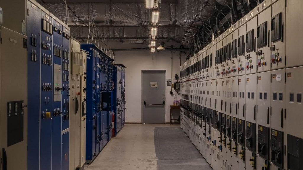
OpenAI has pledged to pay the full cost of the electricity its facilities consume, along with the infrastructure upgrades required to supply them. It also proposes financial safeguards to prevent households and businesses from bearing costs if a planned project is delayed, scaled down or cancelled.
The company has proposed reducing electricity consumption during periods of peak demand and making power available to the grid when necessary. Its planned facility in Effingham County, Georgia, illustrates this approach. Under an agreement with Georgia Power, the utility can reduce electricity supplied to the facility by up to 1,000 megawatts during periods of peak demand.
Water Consumption and Environmental Disclosure
Cooling systems are another environmental concern. Data centres generate considerable heat, and some cooling technologies require substantial quantities of water to maintain operating temperatures. OpenAI says it will prioritise closed-loop and low-water cooling systems and develop water-management plans for individual facilities. It has also committed to publishing site-level information on electricity and water consumption.
The company plans to disclose construction details and commission independent noise studies before facilities begin operations. Annual reporting on relevant environmental impacts is also part of the compact. These disclosures could help communities assess the pressures associated with hosting large computing facilities. Their usefulness, however, will depend on the completeness of the information and the scope for independent scrutiny.
Growing resistance to data centre expansion
The announcement comes as opposition to data centre development gains momentum in the United States. Residents have questioned whether the economic benefits of hosting these facilities justify their demands on local electricity, water and infrastructure. According to Data Center Watch, at least 45 data centre projects worth 68 billion dollars faced disruption from local opposition during the second quarter of 2026.
OpenAI has also promised to publish local hiring goals and provide information about employment opportunities. Its commitments include helping local suppliers compete for contracts and encouraging partnerships with community colleges and trade organisations to prepare workers for construction and technical jobs.
However, voluntary corporate commitments do not carry the same force as legally enforceable regulations. OpenAI’s policy blueprint therefore calls on governments to establish stronger oversight of electricity costs, environmental disclosures and community benefits.
As AI computing demand continues to grow, the pressure on electricity networks, water resources and local infrastructure is likely to intensify. Whether OpenAI’s compact delivers meaningful accountability will depend on how consistently its commitments are implemented and independently scrutinised.
Technology
How an Indian-made Silicon Chip Could Help Terahertz Signals Overcome Obstacles in Future 6G Networks
An Indian research team at JNCASR has demonstrated a silicon photonic chip that allows terahertz signals to cross engineered barriers with minimal loss, a development that could advance high-speed circuits for future 6G networks.

A sharp bend, a junction or a sudden change in a circuit’s structure can weaken an electromagnetic signal. When communication systems operate at increasingly high frequencies, even these seemingly small disruptions become significant engineering obstacles. For researchers working towards sixth-generation (6G) wireless technology, finding ways to guide signals through compact circuits without losing their strength is a growing challenge.
A research team in India has demonstrated an approach that could help address this problem. Using a specially engineered silicon chip, scientists at the Jawaharlal Nehru Centre for Advanced Scientific Research (JNCASR), Bengaluru, have shown that terahertz waves can cross artificial barriers with very little signal loss, even while carrying high-speed data.
The work draws on a phenomenon called photonic Klein tunnelling, which describes how waves can pass through certain barriers without undergoing the substantial reflection or attenuation commonly associated with such obstacles.

In one of the three devices developed by the researchers, data transmission reached 100 gigabits per second (Gbps). The findings, published in Advanced Materials, offer a potential design approach for the compact terahertz circuits that future communication technologies may require.
Borrowing a Principle From Quantum Physics
The idea behind the research has its origins in a phenomenon associated with quantum mechanics. In quantum physics, Klein tunnelling describes the unusual ability of certain particles to pass through a potential barrier even when classical physics would predict that they should be reflected. Researchers have explored analogous behaviour in photonic systems, where electromagnetic waves can exhibit similar transmission characteristics.
The JNCASR team applied this principle through topological photonics, a field concerned with controlling the movement of electromagnetic waves using specially designed structures. They created a silicon photonic crystal resembling the honeycomb lattice of graphene, with triangular holes arranged in a precise pattern across a silicon slab. This arrangement produces boundary channels along which terahertz waves can propagate. These channels are resistant to certain forms of backscattering, helping signals retain their direction of travel.
The researchers then introduced artificial obstacles into these pathways by changing the dimensions of the triangular holes over a short section of the crystal. The experiment tested whether the waves could retain their transmission characteristics even when their pathways were deliberately disrupted.
When a Barrier Barely Interrupts the Signal
The results showed that the engineered structures could transmit terahertz waves across the barriers with remarkably little loss, provided the strength of the barrier remained below a characteristic coupling threshold of the crystal. A single barrier produced only about 1–2% signal loss. Even with two barriers placed consecutively, the loss remained around 2–3%. For comparison, a similar barrier in a conventional, non-topological waveguide caused a considerably greater reduction in transmission.
This is significant for circuit design because communication signals must often navigate multiple pathways and changes in geometry within a limited physical space. Reducing the losses associated with these obstacles could give researchers greater flexibility when designing compact terahertz components.
The team demonstrated the principle in three silicon devices. One incorporated two barriers in sequence. Another used an omega-shaped pathway containing four sharp bends and a central barrier. The third was a power splitter, which divided an incoming signal into two branches, with one branch containing an engineered barrier.
The devices were fabricated using high-resistivity silicon, a material compatible with established semiconductor manufacturing processes. Measurements across frequencies of 310–360 GHz closely matched the researchers’ computer simulations. In the power splitter, the two output signals remained nearly identical, indicating that the barrier had little effect on signal transmission.
What does 100 Gbps Mean in Practice?
The researchers also examined whether the structures could carry high-speed data, rather than simply transmit terahertz waves. The double-barrier device achieved a data rate of 48 Gbps, while the omega-shaped configuration supported 60 Gbps. The power splitter recorded the highest rate, reaching 100 Gbps using QAM-32 modulation. This technique encodes information through variations in the amplitude and phase of a signal.
At 100 Gbps, a five-gigabyte high-definition film could theoretically be transferred in less than half a second. The different transmission rates are important because they show how the approach performed across three distinct circuit configurations. The 100 Gbps result was achieved by the power splitter, rather than all three devices. The demonstration suggests that engineered barriers need not substantially compromise data transmission, even in circuits incorporating multiple pathways and sharp bends.
From a Laboratory Demonstration to Future 6G Hardware
Terahertz frequencies, which lie between microwaves and infrared light in the electromagnetic spectrum, are attracting interest for their capacity to support high-bandwidth communication. Their potential lies in accommodating large volumes of data at speeds that conventional wireless technologies may struggle to sustain. However, generating and transmitting terahertz signals is only part of the challenge. Researchers must also develop components capable of directing, dividing and processing these signals within compact devices.
The JNCASR study addresses this less visible aspect of future communication infrastructure. Its findings could help in developing integrated terahertz circuits that route and split signals on a single chip without substantial transmission losses. The next step for the research team is to explore whether the engineered barriers can be adjusted electrically, thermally or mechanically. This could eventually allow a device to redirect signals between different pathways on demand, potentially enabling more adaptable terahertz circuits.
The work remains an experimental demonstration of signal transmission at the chip level; it does not establish a commercially deployable 6G system. Further research will be needed to integrate these components into larger communication architectures.
Led by Abhishek Kumar, Assistant Professor at JNCASR and head of its Meta Optics Laboratory (MetoLab), the study involved joint first authors Samina Mulla and Sangram Kumar Sadhu. Researchers from JNCASR, IISER Kolkata, IIT Bombay, the Institute of Microelectronics at A*STAR, Singapore, and the University of Lille and CNRS, France, also contributed. The research offers a new way of thinking about how high-frequency signals can be guided through increasingly intricate circuits. As work on 6G progresses, such advances in the underlying hardware will help determine how much of the promised speed and bandwidth can eventually be translated into practical communication systems.
Technology
India Unveils Three Homegrown AI Models, Covering 22 Indian Languages
India has released three indigenous AI models under the IndiaAI Mission. EKA-1 supports all 22 scheduled Indian languages, while Dhīr 2B and Dhīr 5B offer multilingual AI assistance with offline deployment capabilities.

India has released three indigenous artificial intelligence models under the IndiaAI Mission, with applications ranging from multilingual reasoning and coding to offline AI assistance in sensitive sectors such as defence, government and education. The models — EKA-1, developed by Soket Labs Technology and Research Private Limited, and Dhīr 2B and Dhīr 5B, developed by ZenteiQ AiTech Innovations, were unveiled in New Delhi under the IndiaAI Innovation Centre (Foundation Models) pillar.
The three models have different technical capabilities and deployment priorities. EKA-1 is designed as a large multilingual foundation model supporting all 22 scheduled Indian languages and English. The Dhīr models, meanwhile, focus on lightweight, locally deployable AI assistance, allowing organisations to process information without depending on continuous cloud connectivity.

EKA-1 Trained on 7.5 Trillion Tokens
Developed by Soket Labs, EKA-1 is a 26.3-billion-parameter foundation model trained on approximately 7.5 trillion tokens. It supports all 22 scheduled Indian languages alongside English and is designed for mathematical tasks, coding, reasoning and agentic applications.
The model uses an open, sparse hybrid architecture. Its intended applications include banking, financial services and cybersecurity, where understanding India’s digital ecosystem and sector-specific requirements is important. According to Abhishek Upperwal, CEO of Soket Labs, the model was developed with support from the IndiaAI Mission to address requirements within India’s banking, financial services and cybersecurity sectors.
Dhīr Models Target Offline and Secure AI Applications
ZenteiQ has introduced two open-source models, Dhīr 2B and Dhīr 5B, supporting English and 10 Indian languages. Their primary focus is secure deployment within organisations. The models can operate on-premise, enabling institutions to use AI systems within their own computing infrastructure rather than relying entirely on external cloud services.
They support document-grounded automation, knowledge retrieval and citizen-facing or enterprise services. The press release identifies defence, government, industrial and educational institutions as potential application areas, particularly in environments with limited internet connectivity or sensitive information.
Their lightweight architecture also allows deployment on mobile devices, according to ZenteiQ. The company says the models can run across different computing platforms, including graphics processing units (GPUs) and tensor processing units (TPUs). Prof. Sashikumar, CEO of ZenteiQ AiTech Innovations, said local deployment would allow users to retain data on their devices, improving privacy and security while reducing dependence on cloud connectivity.
Public Computing Infrastructure Supports Model Development
Both development teams were selected under the IndiaAI Innovation Centre pillar, which aims to build indigenous foundation models and large language models. The IndiaAI Mission provided access to subsidised national AI computing infrastructure and support for associated research expenses. These resources helped the selected teams develop their models.
Speaking at the launch, S. Krishnan, Secretary of the Ministry of Electronics and Information Technology, said indigenous AI models could strengthen India’s technological and strategic autonomy while creating opportunities to improve productivity across government, industry, research and education. He also pointed to AIKosh, the IndiaAI datasets platform, as a channel through which researchers, students, innovators and the wider public could access these resources and experiment with AI applications.
India’s Wider AI Development Programme
Approved by the Union Cabinet on March 7, 2024, the IndiaAI Mission operates through seven pillars: computing capacity, the Innovation Centre, the AIKosh datasets platform, application development, future skills, startup financing, and safe and trusted AI. The development of EKA-1 and the Dhīr models falls under the Innovation Centre pillar, which supports the creation of foundation models tailored to India’s requirements.
The models represent two different approaches to expanding domestic AI capabilities: large-scale multilingual processing and lightweight AI systems designed for secure local deployment. Their practical impact will depend on how effectively they perform across real-world applications and how widely organisations adopt them.

Why NVIDIA Matters to the AI Revolution as Leadership Crisis Rocks the Chipmaker

MIT Develops AI Technique to Make Climate Predictions Faster and More Reliable

Global Climate Finance Hits Record $1.9 Trillion, but Vulnerable Nations Continue to Face Adaptation Funding Gap

India Ranks 28th in Global Climate Ranking, Down Five Places

Global fossil fuel emissions projected to fall in 2026, but India’s emissions to rise 4.4%

Indian universities lead Asia in research output per faculty, but the country’s top six all slip in QS ranking

Europe Braces for Extremes as Commission Unveils Climate Resilience Framework

Why Delhi’s Geography Makes It Vulnerable to Severe Air Pollution

Delhi’s Air Quality Paradox: Lower Average, Higher Everyday Pollution

NMC Directs Medical Colleges to Set Up Patient Safety Committees
-

 Math4 months ago
The 2026 Fields Medals: Four Proofs, Four Decades-Old Problems Solved
-
EP Deep Dive: Data & Solutions4 months ago
After Kerala’s Deadliest Landslide, the Hardest Thing to Rebuild Was Childhood
-
EP Deep Dive: Data & Solutions4 months ago
West Asia Crisis: Can Kerala’s Returning Gulf Migrants Find a Future in the Green Economy?
-
Space & Physics6 months ago
India Semiconductor Mission: ‘It’s Not About Fabs. It’s About Building An Entire Ecosystem’
-
Interviews2 months ago
From Scams to Screens: How the National Stock Exchange Rewrote India’s Equity Story
-
Climate & Environment5 months ago
The Climate World Cup? How Climate Change Could Affect Player Performance at the 2026 World Cup
-
Society4 months ago
What Is Civilisational Diplomacy? Understanding India’s Newest Foreign Policy Tool
-
Society5 months ago
From Bell Labs to the Classroom: A Second Career in Teaching