Space & Physics
M P Parameswaran: The Scientist Who Took Science to the People
M. P. Parameswaran, who died aged 91 on August 11, 2026, spent decades taking science beyond laboratories through KSSP, Malayalam science writing, literacy campaigns and environmental activism.

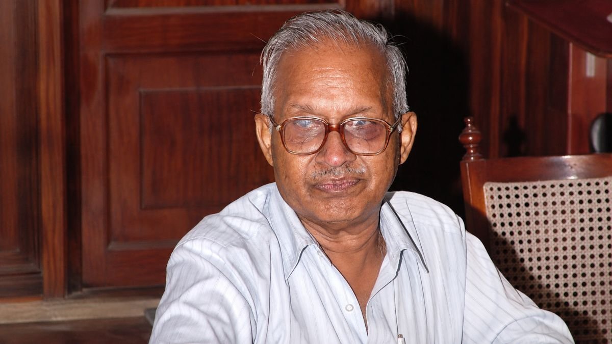
M P Parameswaran, who died on 11 August 2026 at the age of 91, spent his life trying to close the distance between scientific knowledge and the people it was meant to serve. Trained as a nuclear engineer, he walked away from India’s atomic establishment in 1975 to build one of the country’s most influential people’s science movements from the ground up.
He leaves behind an unusual body of work spanning nuclear science, science writing, literacy, language technology, environmental activism, rural development and political thought.
What connected these seemingly disparate pursuits was a single conviction: science should not remain confined to experts. Scientific knowledge, he argued through his work, had to become accessible enough for ordinary people to understand, question and participate in decisions affecting their lives.
From Nuclear Science to People’s Science
Parameswaran was born on 18 January 1935 in Kiralur (Kiraloor), a village in Thrissur district then part of the princely state of Cochin. He graduated in electrical engineering from the College of Engineering, Thiruvananthapuram, in 1956, before travelling to the Soviet Union, where he earned a doctorate in nuclear engineering from the Moscow Power Engineering Institute in 1965. He joined the Bhabha Atomic Research Centre (BARC), India’s premier nuclear research institution, in 1957 and remained there until 1975 — becoming part of the scientific establishment building the foundations of India’s nuclear programme.
But the work that made him a public intellectual began when he left the laboratory.
In 1975, Parameswaran resigned from BARC and joined the Kerala Sasthra Sahithya Parishad (KSSP). The move changed the direction of his life. KSSP had begun as a forum of science writers but evolved, with Parameswaran among its central figures, into a much broader people’s science movement. Under his involvement, science communication became connected with literacy, health, environment, technology and development.
He helped take science out of laboratories and classrooms and into public spaces — through books, magazines, campaigns, village meetings and travelling programmes.
Language was Central to This Effort
Parameswaran wrote extensively in Malayalam, Kerala’s regional language, producing popular science books and hundreds of articles on subjects including nuclear science, astronomy, mathematics, ecology and social science. His contribution was not simply to translate scientific concepts; he helped establish Malayalam as a language in which scientific ideas could be discussed with a wider public.
His interest in accessibility even extended to technology itself. Between 1969 and 1973, while on deputation from BARC, he served as Assistant Director of the State Institute of Languages in Kerala. During this period he was involved in developing a Malayalam keyboard layout for typewriters — work later associated with the development of the INSCRIPT keyboard layout used in Indian-language computing today.
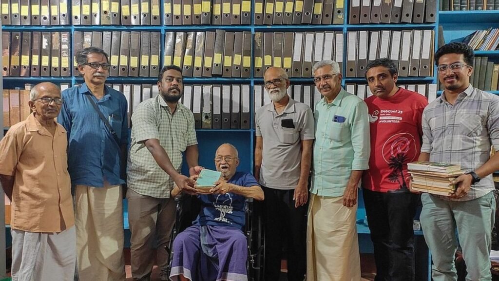
It was a small but revealing example of his approach: technology had little value if people could not use it.
Building a National People’s Science Movement
Parameswaran’s contribution went beyond writing. He played a major role in taking the people’s science movement beyond Kerala. In 1987, as convener of the National Organising Committee, he was central to the Bharat Jan Vigyan Jatha, a nationwide science communication campaign that took scientific ideas to communities rather than waiting for audiences to come to scientific institutions. He was also instrumental in establishing the All India People’s Science Network, bringing together people’s science organisations from across the country.
These initiatives changed the scale of science communication. It became not merely the work of individual writers explaining discoveries, but an organised effort to build public engagement with science.
Literacy As Participation
The same philosophy shaped Parameswaran’s work in literacy. He played an important role in the Total Literacy Campaign in Ernakulam, in which KSSP worked with the district administration to take literacy beyond conventional classroom structures. The experience later became an important model for India’s national literacy campaign.
In 1990, he was also instrumental in organising the Bharat Gyan Vigyan Jatha in support of the National Literacy Mission, a movement that eventually contributed to the formation of the Bharat Gyan Vigyan Samiti.
For Parameswaran, literacy and scientific awareness were closely related. Knowing how to read was only the beginning; people also needed the ability to examine information, weigh evidence and participate in public decisions.
When Science Met Development
Parameswaran’s questions became more difficult when he began examining the consequences of technology itself. He increasingly focused on appropriate technology, rural development, decentralisation and environmental sustainability, and was associated with the Integrated Rural Technology Centre.
He was also a central figure in two of Kerala’s defining environmental campaigns: the movement against the Silent Valley hydroelectric project, which helped save one of India’s last untouched rainforests, and the later opposition to the Athirappilly hydroelectric project. Both battles shaped his conviction that development decisions could not be left to engineers and planners alone.
The Bhopal gas disaster of 1984 sharpened these concerns further. It demonstrated that scientific and industrial advances could produce enormous social and environmental risks when technological decisions were made without adequate attention to safety and public accountability. For Parameswaran and the people’s science movement, the lesson was not to reject science or technology but to ask harder questions about their use: Who benefits? Who bears the risks? And who gets to decide?
Questioning the Idea of Progress
His intellectual journey eventually took him beyond science communication into a broader critique of development. In his book Fourth World: Dream and Reality, Parameswaran set out an alternative model built around decentralisation, ecological sustainability, democracy and a critique of consumerism. The “Fourth World” thesis brought him into sustained conflict with the Communist Party of India (Marxist), or CPI(M), to which he had long belonged, and ultimately led to his expulsion from the party.
His political conclusions remain a subject of debate. But they reveal an important feature of his intellectual life: he was willing to question established ideas of progress, including those within his own political tradition. He later reflected on that journey — from young engineer in Moscow to nuclear scientist, people’s science activist and Marxist theorist who found himself outside the party he had served for decades — in his Malayalam autobiography, Kaalaharanamillatha Swapnangal (Timeless Dreams).
For Parameswaran, development could not simply be measured by economic growth or technological advancement. It also had to be judged by its effects on people, communities and the environment.
Recognition
Parameswaran’s writing and activism were recognised early and late in his career. He received the Books for Neoliterates Award in 1962, the Basic and Cultural Literature Award in 1964, and the Children’s Literature Award in 1984. In 2022, the Government of Kerala honoured him with the Kerala Sree Award, the state’s third-highest civilian award, for his lifetime contribution to science and society.
Science Without Silos
Parameswaran’s contributions are spread across several fields. He helped build KSSP into one of India’s most influential people’s science movements. He helped establish national networks for science communication. He wrote extensively in Malayalam and brought scientific subjects into public discourse. He contributed to language technology. He played important roles in literacy campaigns that reached far beyond Kerala. He helped shape landmark environmental struggles. And he became a prominent critic of environmentally and socially unsustainable models of progress.
But reducing his legacy to this list would miss what made these contributions part of the same story. Parameswaran did not see science as a body of knowledge that moved in one direction — from laboratories to the public. He saw it as something that should enable people to participate. That is why his career could move so naturally from nuclear research to Malayalam publishing, from science campaigns to literacy, and from technology to questions of ecology and democracy.
His relevance may be even clearer today. Artificial intelligence, biotechnology, climate change, nuclear energy and public health increasingly shape everyday decisions, while the knowledge needed to understand them often remains concentrated among specialists. Parameswaran spent much of his life trying to narrow that distance.
He began by working with some of India’s most sophisticated scientific technologies. He ended up devoting his life to a more fundamental question: how can scientific knowledge become part of public life without losing its rigour — and without leaving the public behind? His answer was not simply to popularise science. It was to make people participants in it.










Space & Physics
World Space Week 2026: How the Rocket Revolution Is Changing Space
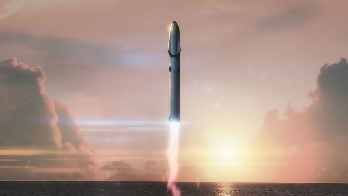
World Space Week 2026 explores the Rocket Revolution, from reusable launchers and private space companies to the growing role of satellites.
Space & Physics
A Dead Star Feeds Off Planet Formed From Its Ashes
It adds to a known coterie of planets now found orbiting dead stars, astronomers are busy studying to spot signs of life.

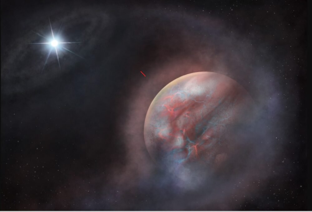
A planet orbiting once every 4 days around a white dwarf star HS 0209+0832 – about 270 light years in the direction of the constellation Pisces – is steadily losing its atmosphere to its host star. While many stars in solar systems beyond our own often feed on their planets, this particular star feeds on its own ashes.
The gaseous planet HS 0209+0832 b was discovered in 2024, when the Transiting Exoplanet Survey Satellite, a NASA space telescope, found it orbiting the white dwarf star over the course of four days. The new study followed through with detailed observations from TESS data, NASA’s space-based Far Ultraviolet Spectroscopic Explorer, in addition to the ESO’s mountain-based Very Large Telescope, to study the star’s atmosphere and in turn inferring some chemistry occurring in the planet.
In a study published in the journal Nature Astronomy on Monday and funded by NASA, European Research Council, Fundación Occident and the Instituto de Astrofísica de Canarias, an international team of astronomers have reported imprints of niobium, a heavy element, in the atmosphere of a white dwarf star.
Astronomers predict the transiting young planet around the dead star is supplying that niobium back to its host. The sighting is evidence of a “second generation” planet, one of many candidates identified over several years, manifesting in a myriad different ways from spent gas ejected in the wake of stellar deaths.
It adds to a known coterie of planets now found orbiting dead stars, astronomers are busy studying to spot signs of life.
What are white dwarf stars?
White dwarves are an exotic stars, and are all that’s left off giant stars shedding their large gaseous skin in violent deaths. Our sun is destined one day to transform into a white dwarf, but only after swelling in size some five billion years from now to become a red giant when it will eclipse past the earth’s orbit. It would take several million years after that for the red giant sun to shed its gaseous exterior to become a white dwarf.
Planets if any, found orbiting these dead stars may have likely migrated from the new solar system’s outer reaches. All that’s left off the progenitor star’s past are imprints of light metals and other elements on the white dwarf’s atmosphere. Such planets have previously been spotted orbiting pulsars, a kind of neutron star, back in 1992. In fact, its discovery had marked the first ever detection of any planet orbiting a star beyond our sun.
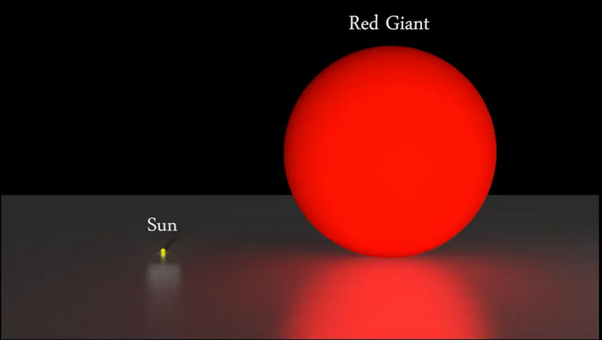
In five billion years, our sun will evolve to become a red giant star. Credit: Svitlana Leonidivna Malchenko
Sighting niobium
Elements such as niobium don’t typically form in the core of stars like our sun. Chemical production usually limits to elements lighter than or until iron, with its 26 protons and 30 neutrons. Beyond that, slamming an extra proton or neutron will cause those to split, leaving iron to be the last element to be directly forged.
Niobium, with 41 protons and 52 neutrons, is thought to be born after absorbing slow passing neutrons when the red giant star dies to form a white dwarf star. This niobium hitches a ride along with rest of the contents of the red giant star, farther into the outer reaches of the system after the formation of the white dwarf.
These contents could create a new disc of circumstellar material with dust and gas that could condense one day to form new planets. The “second generation” planet found orbiting the white dwarf star from the new study, could have been born this way.
Alternatively, it may have been a planet in the outskirts like Neptune, migrating inwards, and enriching itself with niobium-rich star material.
Either way, the planet got too close to its host star, which is irradiating its newfound niobium-rich atmosphere, stripping it away and devouring it.
While it’s likely not a candidate planet for life as we know it to be found, it’s discovery can help ascertain how such worlds are formed in the aftermath of a star’s various phases of evolution.
Space & Physics
Artemis Accords Reach 76 Countries: What It Means for India
The Artemis Accords now have 76 signatories. With NASA inviting ISRO to its Moon Base programme, India’s role in lunar exploration is expanding.
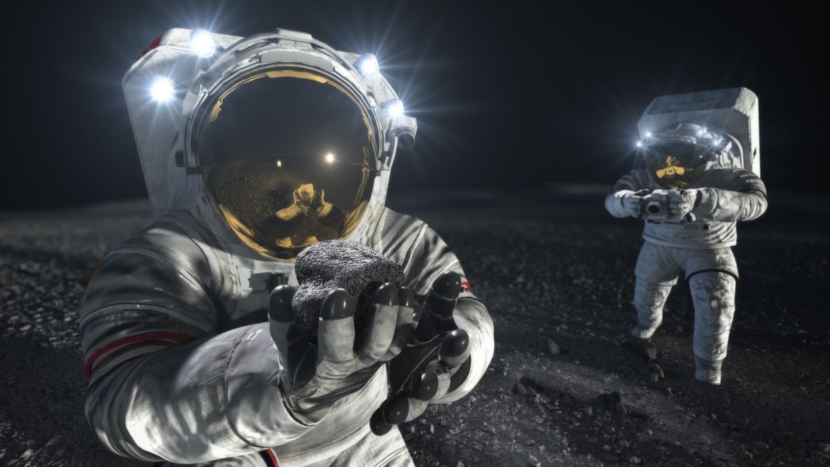
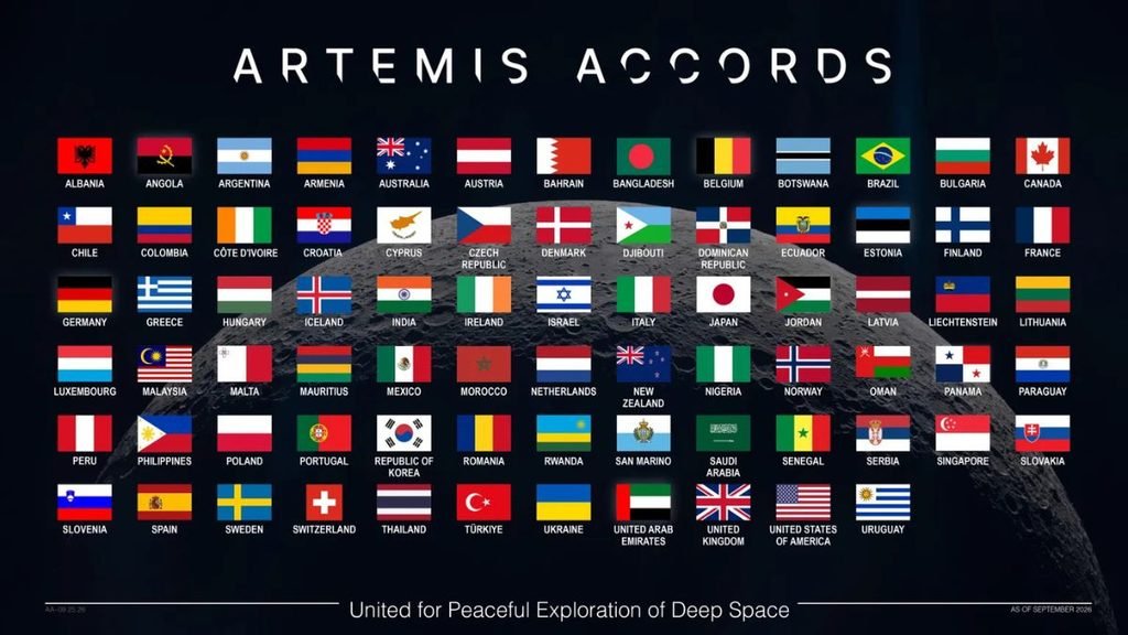
The Artemis Accords now have 76 signatories, expanding the international framework around the next phase of lunar exploration. For India, the milestone comes weeks after NASA invited the Indian Space Research Organisation (ISRO) to participate in its planned Moon Base programme.
Albania, Croatia, Côte d’Ivoire and San Marino joined the Accords in September, taking participation to 76 countries. NASA says nearly 40% of the world’s nations are now part of the framework, which sets principles for peaceful, transparent and responsible exploration of the Moon, Mars and beyond.
India became the 27th signatory in June 2023. At the India-US Civil Space Joint Working Group meeting in Bengaluru in August, NASA invited ISRO to participate in its Moon Base programme. The two countries also agreed to advance discussions on open scientific-data sharing under the Accords.
India’s Moon Base opportunity
The invitation does not specify what India will contribute. NASA has said every Artemis Accords signatory can participate through scientific payloads, technology demonstrations, CubeSats and other capabilities. Any specific Indian contribution would require further agreements.
India, however, is developing its own increasingly ambitious lunar programme. ISRO’s Chandrayaan-4 is planned as a lunar sample-return mission, designed to collect samples from the Moon’s polar region and bring them back to Earth. Chandrayaan-5/LUPEX, being developed with Japan’s JAXA, will study lunar polar volatiles in situ.
These missions could give India experience and scientific capabilities relevant to a future international lunar infrastructure.
ISRO Shaping the Data Conversation
Scientific data could be another area of Indian participation. In May 2026, ISRO led an initial Artemis Accords discussion on advancing open-data practices. NASA subsequently held two workshops focused on making lunar scientific data more accessible, interoperable and reproducible across countries.
That is significant as more lunar missions target the same regions. Shared standards could allow researchers to combine observations from different spacecraft instead of treating each mission’s data separately.
Moon – Space Coperation
India-US space cooperation is also expanding into human spaceflight. ISRO’s 2025–26 annual report records that Indian astronaut Shubhanshu Shukla travelled to the International Space Station in June 2025 as part of the Axiom-4 mission and conducted seven microgravity experiments. ISRO also held discussions with NASA on potential cooperation related to Gaganyaan.
The Artemis relationship therefore sits alongside an existing programme of India-US cooperation, including the NASA-ISRO Synthetic Aperture Radar (NISAR) mission.
What Changes for India?
The significance of the 76-country milestone lies in the network developing around it. The Artemis Accords cover scientific-data sharing, interoperability, non-interference between missions, emergency assistance and protection of historically significant lunar sites. NASA says signatories are now working through technical meetings and workshops to put these principles into practice.
For India, that creates several possible avenues: contributing technology or science to NASA’s Moon Base effort, sharing lunar data, and working with a growing group of countries on standards for increasingly crowded lunar operations. What India’s specific contribution to the Moon Base remains undecided. But with Chandrayaan-4, LUPEX and its human-spaceflight programme advancing alongside deeper NASA cooperation, India is entering the next phase of lunar exploration with its own capabilities already taking shape.


Heatwaves are Affecting Fertility Traits in Bees.

Why Some People Age Better Than Others May Be Written in Their Blood

AI Models Could Soon Spread Across Smart Devices, Raising Cybersecurity Fears

WHO Urges Lifestyle-first Approach as 170 Million Children and Adolescents Live with Obesity

Centre Asks States to Ensure Hospitals Display Service Charges

From Scams to Screens: How the National Stock Exchange Rewrote India’s Equity Story

Knowing When to Think for Ourselves: AI, Intuition and the Education of Discernment

Two Chemists Win Nobel Prize for Solving a Century-Old Puzzle: Why Life Picks One Hand Over the Other

After a Scorching Summer, Delhi’s Children Are Slow to Return Outdoors

India’s AI Moment Rests on More Than Code
-

 Math3 months ago
The 2026 Fields Medals: Four Proofs, Four Decades-Old Problems Solved
-
EP Deep Dive: Data & Solutions3 months ago
After Kerala’s Deadliest Landslide, the Hardest Thing to Rebuild Was Childhood
-
EP Deep Dive: Data & Solutions3 months ago
West Asia Crisis: Can Kerala’s Returning Gulf Migrants Find a Future in the Green Economy?
-
Space & Physics5 months ago
India Semiconductor Mission: ‘It’s Not About Fabs. It’s About Building An Entire Ecosystem’
-
Interviews3 weeks ago
From Scams to Screens: How the National Stock Exchange Rewrote India’s Equity Story
-
Climate4 months ago
The Climate World Cup? How Climate Change Could Affect Player Performance at the 2026 World Cup
-
Society3 months ago
What Is Civilisational Diplomacy? Understanding India’s Newest Foreign Policy Tool
-
Society4 months ago
From Bell Labs to the Classroom: A Second Career in Teaching