Connect with us

Space & Physics

Ancient Martian Valleys Reveal Gradual Climate Shift From Warm And Wet To Cold And Icy: Study

A new study led by researchers at IIT Bombay has provided fresh evidence showing how Mars gradually transitioned from a warm, water-rich planet to a cold, icy world

Published

on

Untitled design 4
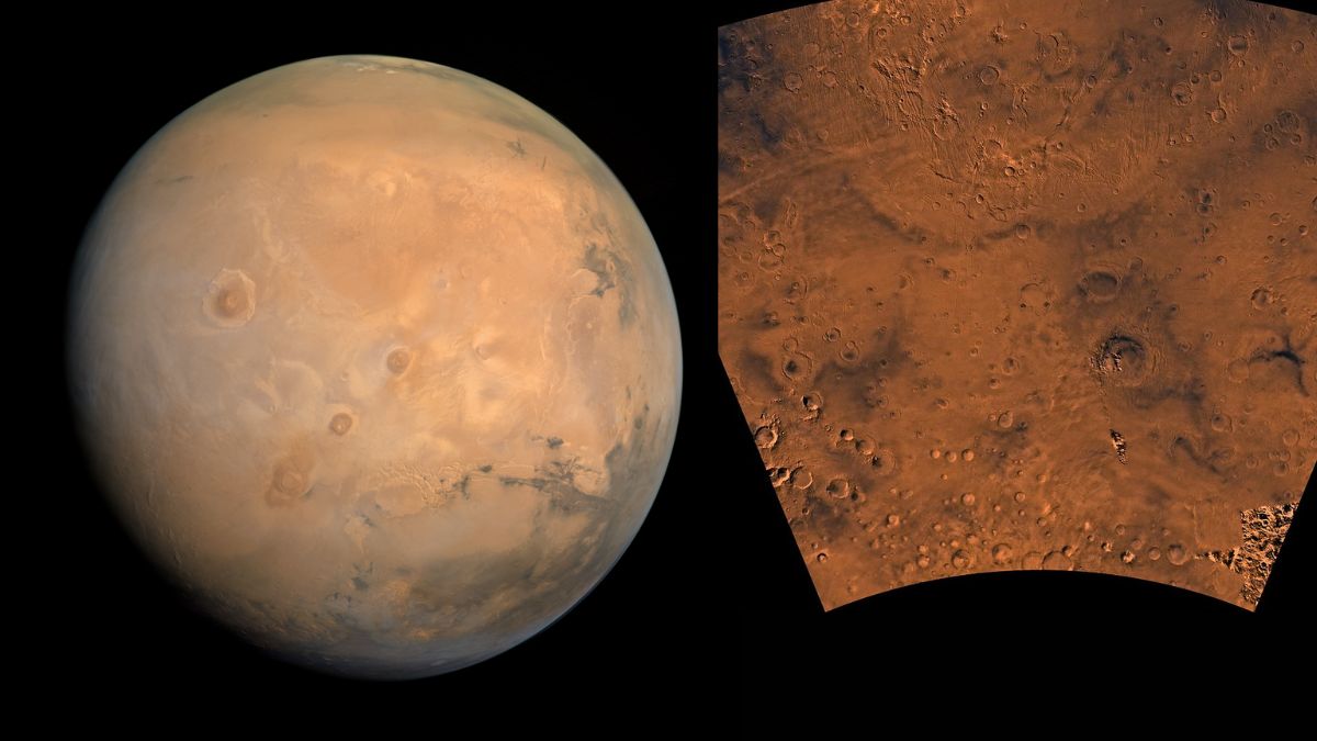
Left: Mars. Credit: Kevin Gill/Wikimedia. Right: Thaumasia region of Mars. Credit: NASA/JPL/USGS

A new study led by researchers at IIT Bombay has provided fresh evidence showing how Mars gradually transitioned from a warm, water-rich planet to a cold, icy world, by analysing ancient valley networks in the Thaumasian Highlands region of the Red Planet.

The findings, based on high-resolution orbital data, suggest that Mars experienced a long-term climate shift—from surface water-driven erosion during the Noachian period around four billion years ago to increasingly glacial and frozen conditions by the Hesperian period, roughly three billion years ago.

“Both these planets started with similar compositions and atmospheres. So, one of the most pressing questions is, where did all that water go, and why didn’t Mars evolve along the same direction as Earth? So, we wanted to find at what stage it lost its water,” said Alok Porwal of IIT Bombay in a statement issued by the institute.

Tracking Mars’ changing climate

The research focused on the Thaumasia Highlands, one of Mars’ most ancient geological regions, which stretches from the equator toward higher latitudes. According to the researchers, this makes it an ideal natural laboratory to study climate-driven geological changes over time.

“The Thaumasia Highlands is a region somewhat like the Indian subcontinent. It extends from the equator to higher latitudes, so it has a range of climates and geographies. It also has both very ancient geologic formations and more recent features, which gives an overall view of the planet,” Porwal said.

The team analysed more than 150 complex valley networks using datasets from NASA’s Context Camera (CTX) and Mars Orbiter Laser Altimeter (MOLA), the European Space Agency’s High Resolution Stereo Camera (HRSC), and ISRO’s Mars Orbiter Camera aboard the Mangalyaan mission. Each valley was carefully mapped to minimise errors caused by natural topographic variations.

Water-carved valleys to ice-shaped terrain

The researchers examined both qualitative and quantitative indicators to identify whether valleys were shaped by flowing water or glacial ice. Features such as fan-shaped sediment deposits and branching valley patterns pointed to fluvial erosion, while moraine-like formations, viscous flow features and ribbed terrain indicated glacial processes.

“When water is flowing, it carries heavy materials at the bottom and cuts the ground vertically. So, the shape it carves is more of a V-shaped valley. Glaciers, which have a mix of ice and debris, are heavier. When they move, they slide over the surface and create a U-shaped valley,” said Dibyendu Ghosh, the study’s first author, in the IIT Bombay statement.

Another key parameter was the angle at which valleys merge.

“When water is flowing, it follows the slope, so two valleys will flow parallel to each other and meet at an acute angle. Glaciers can move laterally, so the angles become more obtuse,” Ghosh explained.

The analysis showed that low-latitude valleys near the Martian equator were primarily shaped by flowing surface water, indicating warmer climatic conditions. In contrast, valleys at higher latitudes displayed increasing signs of fluvioglacial activity, suggesting a colder environment where ice played a growing role.

Evidence of frozen subsurface water

The study also supports the idea that much of Mars’ surface water gradually retreated underground as the planet cooled.

According to the researchers, valley formation peaked during the Noachian period between 4.1 and 3.7 billion years ago, declined during the transition to the Hesperian, and later showed stronger signatures of glacial modification and groundwater erosion.

Future exploration

While the findings offer a more coherent picture of Mars’ climatic evolution, the team noted that linking valley networks precisely to subsurface structures and geological timelines remains challenging.

Looking ahead, Porwal emphasised the need for more advanced missions to refine the planet’s climate history. “If I had a chance to suggest (for a future Mars mission), I would recommend a lander to get more geophysical data. And an orbiter with high-resolution imaging and infrared imaging capabilities to thoroughly study its geological history,” he said.

Space & Physics

India Semiconductor Mission: ‘It’s Not About Fabs. It’s About Building An Entire Ecosystem’

India Semiconductor Mission is reshaping the country’s chip ambitions. Neelkanth Mishra explains the opportunities, challenges and long-term strategy.

Dipin Damodharan

Published

on

Neelkanth Mishra, Chief Economist at Axis Bank and member of the India Semiconductor Mission advisory committee, speaking about India's semiconductor ambitions and chip ecosystem.
From extreme ultraviolet lithography to the economics of fabrication, semiconductors sit at the intersection of advanced science and industrial complexity. Neelkanth Mishra unpacks where India stands today, the constraints it faces, and the strategic choices that will define its place in the global chip ecosystem. Image: Dipin Damodharan/EdPublica
India Semiconductor Mission is at the centre of the country's efforts to build a globally competitive chip ecosystem
Photo by Christian Wiediger/Unsplash

Let me start with asking something out of curiosity – how did you get interested in semiconductors in the first place?

When I joined Credit Suisse First Boston in 2003 in Singapore, the person who hired me was heading Asia technology research and was also the lead analyst for semiconductor foundries such as TSMC and UMC. I was hired to cover IT services, but he wanted help in building the semiconductor research franchise.

That led me to start reading about how chips are made. At that time, the industry was transitioning from 130-nanometer to 90-nanometer nodes, and copper was being introduced to replace aluminum due to resistance issues. There were challenges around yields because copper was seeping into substrates. I remember writing my first note around this issue after going through technical papers.

ep subscription
Subscribe to Education Publica, India’s only global magazine on science and education, and support independent science journalism.

That note became quite popular, and it gave me the confidence to continue covering semiconductors. I spent a lot of time travelling to Taiwan, studying DRAM cycles, capex cycles, node transitions, and the broader global semiconductor ecosystem. Eventually, I moved to Taipei and began covering chip design companies such as MediaTek.

j2 6

At that time, were you also tracking what was happening in India?

India has had chip design activity for a long time, even in the 1990s. Companies like Texas Instruments, Cadence, and Synopsys were recruiting from Indian campuses. Many engineers built long careers in these firms.

However, India did not have domestic chip manufacturing or strong Indian-owned chip design companies. By the mid-2000s, global firms such as Nvidia, Broadcom, and Intel began setting up design centres in India. So the design ecosystem was growing, but it was largely driven by global companies.

It is only in the last four to five years that more serious efforts have begun toward building Indian-owned capabilities.

So what changed in the last few years? Was it policy, or something else?

Policy has played a role. The Design Linked Incentive (DLI) scheme has been an important catalyst. We are seeing some early success. At the same time, there is also an evolutionary factor at play. Engineers who moved abroad 20–25 years ago are now at a stage where they have both the experience and financial capacity to take entrepreneurial risks. Many also want to return to India.

j5 5

Another important factor is the growth of India’s electronics manufacturing ecosystem. As assembly volumes increase, there is greater awareness of what products need to be designed. Without that visibility into OEM pipelines, it is difficult to design chips.

Schemes like PLI for electronics manufacturing have helped build that awareness and ecosystem. As downstream industries grow, upstream opportunities in chip design also become clearer.

As US is good at designing chips, Taiwan and South Korea are good at manufacturing There’s always this question – should India focus on design, manufacturing, or packaging?

There is no either/or. India needs to participate across the value chain.

We already have a natural advantage in chip design, with about 20% of global design engineers based in India. Design is also less capital-intensive compared to manufacturing. In a $10 chip, $5–6 of value is captured by the designer, and in some cases even more.

At the same time, semiconductor manufacturing is a geopolitical necessity. It is not just a commercial issue but also a matter of national security. That is why governments provide significant subsidies for fabs.

j4 6

However, manufacturing is a low-return business globally. Only a few companies like TSMC and Samsung have consistently generated returns above their cost of capital. Much of the value in the ecosystem is captured by design firms and by capital equipment suppliers, which operate in highly concentrated markets.

Therefore, India must build capabilities across the chain—from design to manufacturing to equipment and materials—if it wants meaningful value capture.

When we talk about building an ecosystem, how complex is that in reality?

It is extremely complex. The industry has multiple layers of specialization. For example, electronic design automation (EDA) tools are dominated by a few companies. Lithography, especially extreme ultraviolet, is controlled by a single company globally. Equipment for deposition, wafer slicing, and testing is also concentrated among a handful of firms.

Even the chemicals used in wafer cleaning are highly sophisticated and require extraordinary purity. A single wafer can take months to manufacture, involving hundreds of process steps.

So when we talk about semiconductors, it is not just about fabs. It is about building an entire ecosystem—equipment, materials, design, testing, and packaging. This is why it is a 15–20 year journey at least.

j7 4
Image credit: Taiwan Semiconductor Manufacturing Co., Ltd

What about talent? Are we ready from a skills perspective?

In general, skilling in India is more of a demand problem than a supply problem. If there is sufficient demand, the industry tends to create the supply.

For example, there is already discussion about developing tens of thousands of chip testing engineers in India, and that is achievable. However, for cutting-edge technologies, there is a need for deeper investment in research.

As we move toward more advanced nodes—such as 7 to 12 nanometers—we will require significant high-end research capabilities. Countries like China took over 25 years to reach that level.

We need to invest not just in near-commercial research (TRL 6–9) but also in fundamental research (TRL 1–4), which creates long-term intellectual property. Government initiatives like the Anusandhan National Research Fund are steps in that direction, but overall R&D spending needs to increase.

What role should industry play in R&D?

Industry participation is essential. The government can catalyse investment, but companies will invest when they see potential returns.

We have seen this in pharmaceuticals, where Indian firms moved into R&D after reaching limits in generics. A similar shift can happen in semiconductors, but it will require scale, capital, and long-term commitment.

j9 1

Where do startups fit into this picture?

Startups will have a significant role, particularly in chip design. Manufacturing is extremely capital-intensive, requiring billions of dollars in investment, which limits the role of startups.

However, in design and innovation, startups can play an important part. Many innovations in the semiconductor ecosystem originate from smaller firms, which are later acquired or integrated into larger companies.

To produce a globally competitive company, you need a large ecosystem of startups, experimentation, and risk-taking.

Coming to policy – what did India learn from ISM 1.0?

ISM 1.0 (India Semiconductor Mission) was a learning curve for everyone. It helped the government understand how to evaluate proposals, support companies, and manage operational challenges.

There were practical issues—from customs procedures affecting sensitive equipment to ensuring uninterrupted power supply. Semiconductor manufacturing requires extremely high reliability, and even a brief power outage can cause significant losses.

Another important learning is that the global industry is now more comfortable working with India. While India may not yet be the first choice, confidence has improved due to visible commitment and progress.

This increased comfort allows India to be more ambitious with ISM 2.0.

j8 3
Photo by Laurel and Michael Evans/Unsplash

How important is policy stability?

Policy continuity is very important because these are long-term projects. Global firms value consistency in decision-making and relationships.

There is also a growing effort to ensure continuity in leadership within government institutions, which helps build expertise and trust over time.

Do we need a dedicated semiconductor research institution like IMEC?

There are existing efforts, such as the facility in Mohali, which supports defence-related applications. There are also discussions around creating IMEC-like research centres.

However, over time, the private sector will need to take a larger role in research. Government support is critical in the early stages, but for sustained innovation and competitiveness, industry-led initiatives are more effective. The government can act as the binding force or the catalyst that brings people to the table; however, I believe it is ultimately better if the private sector takes the lead. This creates a natural incentive for innovation and rigorous research. Beyond a certain point, government support becomes both fiscally unfeasible and operationally undesirable

j10 1

If we look ahead 20 years, where do you see India?

On the design side, India can become much more significant. It is possible to see 10–15 large chip design companies and many smaller firms emerging.

On the manufacturing side, we could have several large fabs and potentially global players establishing operations in India, especially if a strong domestic design ecosystem develops.

For example, companies like TSMC tend to follow innovation ecosystems. If Indian design firms grow in scale and sophistication, it could attract global manufacturing investments.

Neelkanth Mishra, Chief Economist at Axis Bank and member of the India Semiconductor Mission advisory committee, speaking about India's semiconductor ambitions and chip ecosystem.

Let me end with this – can India produce a company like Nvidia?

It is possible, but it requires a large ecosystem. Many Indians already occupy senior roles in global semiconductor companies and are involved in cutting-edge design work.

To create a company of that scale, you need risk capital, entrepreneurial ambition, and a large number of startups. In other markets, hundreds of firms compete, and one eventually emerges as a dominant player.

So it is not about a single effort—it is about building an ecosystem where many experiments take place, and success emerges from that.

Continue Reading

Space & Physics

India’s First Private Theoretical Physics Institute Bets on Curiosity-Driven Research

India’s first private theoretical physics institute aims to strengthen fundamental research and scientific excellence through philanthropy

Published

on

Abhishek Lodha and theoretical physicist Jainendra K. Jain during the launch of the Lodha Theoretical Physics Institute, India's first privately funded centre for theoretical physics research

India’s first privately funded Theoretical Physics Institute signals a new approach to research

As India seeks to strengthen its scientific capabilities and emerge as a developed nation by 2047, a new initiative is testing whether private philanthropy can play a larger role in advancing fundamental science.

The Lodha Foundation has launched the Lodha Theoretical Physics Institute (LTPI), which it describes as India’s first fully privately funded institute dedicated exclusively to theoretical physics research. The institute aims to support long-term, curiosity-driven scientific inquiry by bringing together leading researchers from India and around the world.

BUY THIS SEMICON SPECIAL MAGAZINE 1
Subscribe to Education Publica, India’s only magazine on science and education and support independent science journalism.

Why a private theoretical physics institute matters

The launch comes at a time when discussions about India’s research ecosystem are increasingly focused on how the country can not only expand scientific output but also build globally competitive institutions capable of producing breakthrough discoveries.

At the heart of the new institute is a belief that transformative technological revolutions often originate from advances in basic science.

Theoretical physics may appear distant from everyday concerns, but history suggests otherwise. Quantum mechanics, once regarded as a highly abstract field, laid the foundation for semiconductors, lasers, modern electronics and many technologies that shape contemporary life. Similar advances in fundamental science continue to influence emerging areas such as quantum computing, advanced materials and next-generation communications.

The Lodha Foundation believes that supporting excellence in foundational research is critical for India’s long-term development.

“At the Lodha Foundation, we believe that pursuing excellence in everything we do is essential to creating the greatest possible impact. Whether it is identifying talented minds across the country and supporting them through transformative programmes, investing in urban sustainability solutions, or fostering innovation and research through institutions such as the Lodha Mathematical Sciences Institute and now the Lodha Theoretical Physics Institute, our goal is to contribute meaningfully to India’s journey towards becoming a developed nation,” said Abhishek Lodha, Trustee of the Lodha Foundation and Managing Director and CEO of Lodha Developers.

The institute will be led by Jainendra K. Jain, one of the world’s leading theoretical physicists and a recipient of the Wolf Prize in Physics. Jain’s pioneering work on composite fermions has significantly advanced the understanding of correlated quantum matter and continues to shape modern theoretical physics.

According to Jain, investment in theoretical physics is ultimately an investment in the future of science and technology.

“Theoretical physics lies at the heart of our understanding of nature. Advances in theoretical physics have historically shaped scientific thought and laid the foundation for transformative developments across multiple fields,” he said.

Theoretical Physics Institute and National Aspirations

Jain also linked the institute’s mission to India’s broader national aspirations.

“If India is to become a developed nation by 2047, it will need strong institutions backed by world-class scientific research infrastructure. In that context, LTPI is a significant step forward, as it is the country’s first fully privately funded institute dedicated to physics research,” he said.

Unlike many research initiatives that focus on short-term outcomes or commercial applications, LTPI intends to create an environment where scientists can pursue ambitious questions over extended periods of time. The institute plans to support focused research programmes, international conferences and collaborations among leading physicists.

Ashish Kumar Singh, Chief Mentor of the Lodha Foundation, said the vision is to create a space where scientific curiosity can thrive without unnecessary constraints.

“The idea is to bring together some of the brightest minds from around the world and give them the freedom to think deeply about physics without constraints. When exceptional minds come together, exceptional outcomes often follow. That is the bet we are making for India,” he said.

The launch also highlights a growing trend in scientific philanthropy. While private funding has long played a role in higher education and healthcare in India, dedicated philanthropic investment in fundamental scientific research has remained relatively limited. Institutions such as LTPI could signal a new model in which private donors complement public investments in building advanced research capacity.

Lodha Theoretical Physics Institute launch

To mark its launch, LTPI is hosting the 10th International Meeting on Emergent Phenomena in Quantum Hall Systems (EPQHS-10), bringing together leading researchers working on quantum matter and condensed matter physics. The event also featured a public lecture by Nobel laureate Klaus von Klitzing, whose discovery of the Quantum Hall Effect transformed precision measurement science.

Whether LTPI ultimately succeeds will depend on its ability to attract top scientific talent, produce influential research and establish itself as a globally respected centre for theoretical physics. But its creation raises a broader question for India’s scientific future: can philanthropy help build the institutions needed to support the next generation of fundamental discoveries?

The answer could have implications far beyond physics, shaping how India invests in knowledge creation and scientific excellence in the decades ahead.

Continue Reading

Space & Physics

Can India Turn Quantum Research Into a Global Deep-Tech Industry?

Quantum innovation in India is accelerating through IISc, startups and new partnerships aimed at turning research into market-ready technologies

Joe Jacob

Published

on

Quantum innovation in India is accelerating through IISc, startups and new partnerships aimed at turning research into market-ready technologies

Quantum innovation in India is gaining momentum as research institutions, startups and investors work to transform scientific breakthroughs into commercially viable technologies. The launch of new initiatives at IISc highlights the country’s growing ambition to become a global leader in deep-tech and quantum entrepreneurship.

India’s ambitions in quantum technology received a fresh boost this month with the launch of the Wadhwani-IISc Innovation Centre and a new startup acceleration platform aimed at supporting quantum entrepreneurs. While the announcements themselves may appear institutional, they point to a much larger question: Can India convert its growing scientific capabilities in quantum technologies into globally competitive companies and products?

The answer could shape the country’s future position in one of the most strategically important technological fields of the coming decades.

Quantum technologies, which include quantum computing, quantum communication and quantum sensing, are expected to transform sectors ranging from cybersecurity and healthcare to finance, defence and advanced manufacturing. Governments across the world are investing billions of dollars to secure leadership in the field, viewing quantum technologies not only as economic opportunities but also as matters of national security.

Quantum Innovation in India Enters a New Phase

India has recognised this potential. In recent years, the government launched the National Quantum Mission, committing significant resources to strengthen research and build indigenous capabilities. Academic institutions such as the Indian Institute of Science (IISc), IITs and specialised research centres have expanded their work in quantum science, while a small but growing ecosystem of startups has begun exploring commercial applications.

Yet the challenge extends beyond scientific research.

India has traditionally been strong in producing scientific talent but less successful in translating laboratory discoveries into scalable products and globally recognised technology companies. Bridging that gap requires a combination of research infrastructure, risk capital, industry partnerships and entrepreneurship support.

Bridging the Gap Between Research and Industry

This is where initiatives such as the newly launched Wadhwani-IISc Innovation Centre seek to make a difference. The centre aims to connect researchers, entrepreneurs and industry partners, creating pathways for technologies developed in laboratories to reach markets. It forms part of the broader Wadhwani Innovation Network, which seeks to strengthen deep-tech commercialisation across Indian institutions.

“Quantum technologies represent one of the most transformative frontiers of science and innovation. Through the Wadhwani-IISc Innovation Centre, Quantum Pitch Fest, and the InQubate platform, IISc is creating a collaborative ecosystem to help researchers and entrepreneurs translate cutting-edge quantum research into scalable technologies and globally competitive ventures,” said B Gurumoorthy, Director of the Foundation for Science, Innovation and Development (FSID), IISc.

The launch coincided with Quantum Pitch Fest 2026, where researchers and startups presented ideas spanning quantum computing, communication and sensing. Such forums are increasingly important because quantum innovation often requires long development cycles, specialised expertise and sustained investment before commercial returns become visible.

For India, the opportunity lies not only in producing scientific publications but also in building intellectual property, manufacturing capabilities and globally relevant enterprises. Countries that succeed in commercialising quantum technologies could gain advantages in secure communications, advanced computing and next-generation sensing systems.

Dr Ajay Kela, CEO and Board Member of the Wadhwani Foundation, highlighted the importance of accelerating this transition from research to impact.

“India has world-class research talent and scientific capability. The next frontier is accelerating the translation of research into scalable products, startups, and societal impact. Through the Wadhwani Innovation Network, we are working closely with leading institutions like IISc to help build stronger innovation ecosystems that can take breakthrough ideas from lab to market faster.”

Former ISRO Chair A.S. Kiran Kumar also stressed that technological progress must ultimately serve societal needs.

“Technology alone is not important; how these technological capabilities are used for developing society and country matters more.”

His remarks reflect a recurring lesson from India’s scientific history. Success stories such as the space programme and nuclear energy initiatives were built not only on scientific excellence but also on long-term institutional support, strategic vision and sustained investment.

Quantum technology may now represent the next chapter in that story.

Whether India emerges as a global leader in the field will depend on how effectively it can connect research laboratories with entrepreneurs, investors and industry. The launch of new innovation platforms at IISc suggests that the country is beginning to build those bridges. The real test, however, will be measured not by the number of research papers published, but by the technologies, startups and industries that emerge from them.

Continue Reading

Trending