Society
As Oppenheimer wins the Oscars, here is an epiphany
We can’t unmix science from politics. They’re intertwined.


Earlier today, Christopher Nolan’s much acclaimed film, Oppenheimer (2023), won 7 awards at the Oscars – including Best Picture, Actor, Supporting Actor, Score, Cinematography, Editing and Director.
And what better moment can there be to discuss threats and fears about the wildest creations of nuclear physics?
Oppenheimer made some seminal contributions in quantum mechanics and in black hole physics. He brought ‘quantum physics to the US’. However, Oppenheimer was also a public intellectual, who dabbled with left wing politics in his younger days. He rose to national prominence after he led Los Alamos National Laboratory as Director, in an effort that saw the US develop and wield nuclear weapons. He forever became known as the ‘father of the atom bomb’, a label that didn’t do anything to stop him spiraling into depression, as he saw his legacy tainted with death and destruction.
Nolan’s movie was a biopic, based on authors Martin Sherwin and Kai Bird’s Pulitzer Prize winning biography, American Prometheus: The Triumph and Tragedy of J. Robert Oppenheimer.
In a scene that shakes you to the core, Oppenheimer (played by Cilian Murphy) imagines seeing the horrific effects of a nuclear bombing on humans. A corpse flash fried, that crumbles upon the lightest touch. People mourning deaths of their loved ones, people vaporized leaving no traces behind. Others left alive with burns, and others vomiting irrecoverably from radiation sickness. Just imagine this is a time when people didn’t even really know what radiation sickness was all about. How many people would’ve dabbled with radioactivity? And now all it takes is one bomb to exact such a devastating toll on human life.
We wonder – who’s accountable for all this? The maker or the master? Or both?

Image of the nuclear detonation in US’ Castle Romeo test in 1954. Credit: United States Department of Energy
Oppenheimer lends an opportunity to assess scientists by holding them at the same pedestal as we do with politicians – especially when they’re prone to serious misjudgment. Oppenheimer thought the best way to demonstrate deterrence was to demonstrate the weapon’s capability. He assumed it wouldn’t proliferate, if they were demonstrated with an attack. ‘They (people) won’t fear it, unless they understand it, and they won’t understand it, until they’ve used it,’ as Cilian Murphy said in the movie. And they did use it.
Did people fear it? Yes and no. On one end there’s the physical damage of it all. But on the other end there came the political chain reaction – with nuclear arsenal stockpiling to record highs during the Cold War. There are still enough nukes around the world to end human civilization many times over.
Frankenstein died, but the monster lives on.
It’s an age-old claim now, as old as the Trinity test itself that it was impossible to stop the nuclear bomb developments. Somebody else or the other would have made it. This is sadly true. However, when we think of science itself – as Isidor Rabbi in the movie (played by David Krumholtz) said, ‘I don’t wish the culmination of three centuries of physics to be a weapon of mass destruction.’ Is science really divorced from political realities? Sure, a nuclear chain reaction isn’t dependent on policy. Of course, but launching an initiative to trigger one surely is. Leo Szilard’s letter sent to US President Theodore Roosevelt, signed off by Albert Einstein, discussed the feasibility of the US wielding a nuclear weapon to deter the Germans. That’s as straightforward as it can get.
It reflects policy change, when Nobel Peace Prize winner and nuclear physicist, Joseph Rotblat claimed General Leslie Groves (who oversaw the Manhattan Project) stating that it was the Soviets who the US seeked to intimidate with the Hiroshima and Nagasaki attacks. And when the Soviets surprised the US by revealing their own sophisticated nuclear program with a growing arsenal, the world locked up in a race for their own weapons. There was a total snafu.
Although Nolan used Sherwin and Bird’s source material as the inspiration for Oppenheimer to be depicted as a Prometheus, he’s also undoubtedly similar to Frankenstein as well.
Frankenstein died, but the monster lives on. What can we learn from all of this? Well, science and society are so intertwined that they both shape each other. The other is we may need to figure out who’s accountable for technological and scientific innovations.
Innovation may not really be unstoppable, if there’s collective action and we decide for ourselves what the world ought to be. Perhaps nuclear holocaust isn’t fictional, but at least we can do something for innovations in our society today.
“I have been interested to talk to some of the leading researchers in the AI field, and hear from them that they view this as their ‘Oppenheimer moment’,” said Nolan in an interview to The Guardian. AI can provide jobs as much as it takes away them, and that’s the challenge of our times. “And they’re clearly looking to his story for some kind of guidance … as a cautionary tale in terms of what it says about the responsibility of somebody who’s putting this technology to the world, and what their responsibilities would be in terms of unintended consequences.”
We’d rather be wise and learn from history, than repeat it. May that lead to an era of responsible innovation.











EP Deep Dive: Data & Solutions
After a Scorching Summer, Delhi’s Children Are Slow to Return Outdoors
Extreme heat and children are the focus of this EdPublica report. Parents in Delhi and Noida explain how rising temperatures, air pollution and changing routines are keeping children indoors.

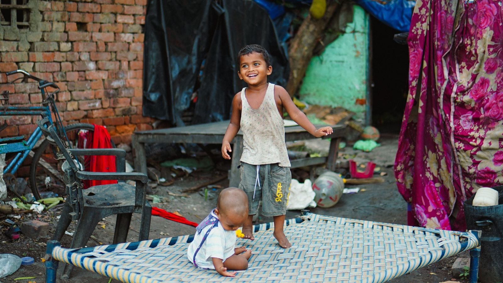
After months of extreme heat, Delhi’s children face another challenge: returning outdoors. Heat, air pollution and changing routines are reshaping how children play. EdPublica spoke to parents in Delhi to understand how extreme heat has changed their children’s play habits and what it might take to bring them back outdoors.
New Delhi: Mohini Bisht is a first-time mother. Her two-year-old son, Shomu (name changed), has just begun to string together his first words. Among the first he learned is “AC” (air conditioner). Living in the National Capital Territory, the family faces daytime temperatures that regularly reach between 42 and 45 degrees Celsius.
“Mummy, garmi lag rahi hai, AC chala do” (“Mummy, it’s hot, turn on the AC”), her son now says. He has learned to turn the AC on and off by himself. On especially humid days, he gets up and flicks the switch on his own.
In April, Delhi saw a maximum of 42.8 degrees Celsius, the hottest for that month in four years. In May, nighttime heat also broke records, with the minimum temperature hitting 32.4 degrees Celsius, the warmest May night in nearly 14 years, according to the India Meteorological Department (IMD).
In June, the heat index, or ‘feels-like’ temperature, soared to 51.3 degrees Celsius, the highest of the year. The heat index combines air temperature and relative humidity to show how hot it actually feels, not just what the thermometer shows.
“The whole day you’re just waiting for evening so you can go out,” Bisht said. As temperatures rose, she stopped taking her son out to play. “If the child gets dehydrated or faces issues, it becomes a big problem,” she said. Her parents and in-laws also advised her not to take him outside.
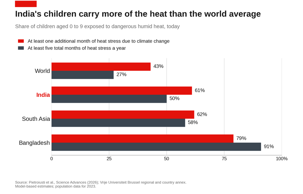
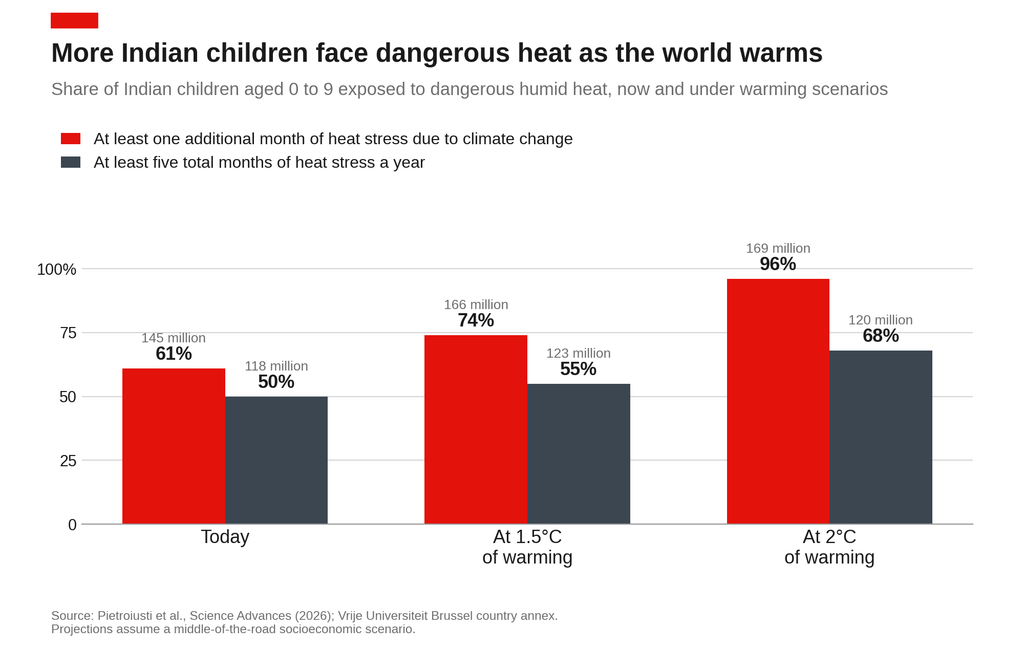
Her caution has a basis. India’s exposure is higher than the global average. Worldwide, up to 560 million children aged 0 to 9, or 43 per cent, live through at least one additional month of heat stress a year because of climate change. In India the share is 61 per cent. For five or more months of total heat stress, the Indian share is 50 per cent, against 27 per cent globally. South Asia is one of the regions with the most children exposed: about 167 million children, or 62 per cent, face an additional month, and in Bangladesh the share is 79 per cent.
Extreme Heat and Children: The Challenge of Outdoor Play
Nearly 145 million Indian children aged up to nine, or 61 per cent of that age group, live through at least one additional month of dangerous heat stress each year because of human-induced climate change, according to a study published in August in Science Advances by researchers led by Vrije Universiteit Brussel. The study estimates that climate change has doubled the number of Indian children facing five or more months of dangerous heat a year, from 59 million to 118 million. The authors note that children are especially vulnerable because their bodies heat up faster than adults’ and regulate temperature less efficiently.
Even as early October brings daytime highs in Delhi that linger in the mid-30s, according to IMD forecasts, summer is retreating from most of north India, bringing the season’s first pleasant evenings. For many families, this raises the question: after months indoors due to oppressive heat, will children return outside?
The challenges don’t end with summer. “Apart from the heat, there is also poor air quality,” said Dr Himani Narula, a development paediatrician in New Delhi. Seasonal illnesses, too, play a role: “Sometimes there is a dengue season and other times there is a flu season.” Parents worry their children will pick up infections, making it hard to let them outside for long. “For all these reasons, children are ultimately at home, even when the weather improves,” she said.
The air is a genuine constraint, not just a parental worry. A 2021 study in Environmental Science and Pollution Research reported an almost 30 per cent rise in daily emergency visits for acute respiratory symptoms among Delhi’s children on high-pollution days. Last winter, the Delhi government suspended outdoor school activities in November and December after the Supreme Court warned against holding outdoor sports in hazardous air.
EdPublica spoke to seven parents from middle-class households in Noida-Delhi, all of whom said they have reorganised their days around the heat, moving their children’s playtime from evening to night to escape gruelling temperatures and humidity. They are not a representative sample, and EdPublica did not measure how much time children actually spend outdoors.
“Dinner is cooked first, then comes the outing, then a late meal and bed. The schedule has changed because of the heat,” said Sunita Kumar, a home tutor and mother of three, including a six-year-old.
Kumar, who lives in Mayur Vihar, New Delhi, worries the routine is changing children’s relationship with the outdoors. “Kids nowadays aren’t seeing the sun,” she said. “They go to school in the morning, stay inside all day, then go home. Even a one-hour tuition is indoors.” This habit, she fears, may outlast the weather. “Kids have built a habit without realising,” she said.
“Kids nowadays aren’t seeing the sun”
The pattern has research behind it. In a 2023 study in JAMA Pediatrics, researchers fitted preschoolers at a university childcare centre in Texas with activity monitors for a week. On hotter days, the children spent more of their outdoor play sedentary, about 70 per cent of it at 35 degrees Celsius against 62 per cent at 22 degrees, and less in moderate-to-vigorous activity, 21 per cent against 27 per cent. The sample was small and the temperatures were milder than Delhi’s summer, but the direction is clear. A 2022 review of more than 150 studies in the journal Temperature also warned that parents’ perception that it is “too hot to play” can further restrict children’s activity.
Moving play to cooler hours is, in fact, what heat-safety guidance advises, alongside hydration and shaded, green outdoor spaces. In that sense, the parents’ adaptation is sensible. The concern is what happens once the heat passes.
The human body and brain tend to acclimatise to repeated exposure of any kind, Dr Narula explained. Keeping children in air-conditioned rooms and away from natural weather, she said, can get their bodies used to the indoor environment and blunt their heat tolerance.
Direct evidence in children is scarce. A small study in Indoor Air compared 20 adults used to air-conditioned and naturally ventilated environments in a climate chamber, measuring skin temperature, sweat rate and thermal comfort. It concluded that long-term exposure to stable air-conditioned environments may weaken thermal adaptability. The study involved adults, not children, and does not show that air conditioning harms a child’s heat tolerance, but it makes Dr Narula’s concern plausible.
But temperature isn’t the only factor shaping how children respond to heat. Bisht notes that her son complains about the heat when alone with her, but behaves differently around friends. “If I bring him with friends or cousins, he plays on the balcony in the sun and enjoys it,” she says. “But if he’s alone with me, he voices his opinions.”
“Children’s tolerance for discomfort changes when other kids are around,” Dr Narula explained. “What the kid is saying is I will accept the discomfort of heat if it means I am enjoying time with peers.” The brain is adapting to these climatic challenges, and according to her, the child needs to get used to this conditioning.
Research on friendship and physical activity points the same way. A 2013 systematised review of friendship networks in the International Journal of Behavioral Nutrition and Physical Activity found that higher activity among friends is associated with higher activity in the individual, and longitudinal studies showed children’s activity shifting to match their friends’. Much of this work is observational, and it is hard to separate influence from children simply choosing similar friends. Still, it hints at what could bring children back outdoors: the company of other children. Parents often tell Dr Narula their kids stay home because there are few other children for them to play with.
Schools, where children already gather, are the obvious place to start, Dr Narula said. Before lessons begin, when the morning heat is lower, children could spend time in the open air, she said: sports, a prayer assembly, physical training, “any kind of activity which children can do with each other in a good setting.”
From toddlerhood through the teenage years, “children look for peers,” something that motivates them far more than being around parents, Dr Narula explained. The outdoors, she said, offers something indoor play cannot, and sunlight helps raise dopamine levels and, with them, mood.
The best-documented benefit of outdoor time in children is for eyesight. A 2024 meta-analysis in Ophthalmic Research found that children and adolescents with the most time outdoors had roughly half the risk of developing myopia of those with the least, and that risk fell as outdoor hours rose: going from 3.5 to 7 hours a week was linked with a 20 per cent lower risk. The leading explanation is that bright outdoor light prompts the retina to release dopamine, which slows the eye’s growth, though the mechanism is not fully settled. Outdoor time did not slow the progression of myopia in children who already had it.
The cooler weeks may be a short window. Whether children use it will depend less on the thermometer than on whether there is anyone outside to play with, and on how long the air stays clear enough to let them.
This article is written as part of the Media Fellowship under the Cities on Fire Initiative in Bangkok, Colombo, Jakarta and Manila and ‘Cooler Cities. Healthier Children. Brighter Futures.’ Initiative in New Delhi.
Health
World Mental Health Day: How Late-Night Scrolling May Be Disrupting Sleep and Fuelling Anxiety
New research is examining how late-night smartphone use, disrupted sleep and passive social media scrolling may be linked to anxiety. Studies highlight the importance of digital habits and bedtime routines in understanding their potential effects on mental health, particularly among young people.


The day often ends with one last check of Instagram, a few minutes on YouTube or a scroll through messages before sleep. But what begins as a brief digital break can stretch late into the night, delaying bedtime and keeping the mind engaged when it should be winding down. Researchers are increasingly investigating whether this pattern of digital exposure, through its effects on sleep, may contribute to anxiety and other mental health difficulties among young people.
As World Mental Health Day is observed on October 10, emerging evidence suggests that the relationship between digital media and psychological well-being may depend not simply on how long people spend online, but also on when and how they use it.
A scoping review published in Computers in Human Behavior Reports in March 2026 examined longitudinal research on social media use and sleep among young people. The review found that approximately 70% of the longitudinal studies examined reported at least one negative association between social media use and sleep outcomes. The most consistent links involved later bedtimes and longer periods spent trying to fall asleep, particularly among those with problematic social media habits or who used platforms at bedtime.
The findings are significant because longitudinal studies track participants over time, helping researchers investigate whether digital habits precede subsequent changes in sleep. However, the authors cautioned that many studies relied on self-reported screen use and sleep patterns, limiting the strength of conclusions about cause and effect.
The review also identified an important distinction: total screen time alone did not consistently predict poor sleep. The timing of use and difficulty controlling online behaviour appeared to matter.
When sleep becomes the missing link
Sleep may help explain why certain patterns of digital engagement are associated with poorer mental health. Notifications, emotionally charged content and the pressure to respond immediately can keep users mentally alert. Scrolling in bed can also displace time that would otherwise be spent sleeping.
Insufficient or disrupted sleep can affect emotional regulation, concentration and the ability to manage everyday stress. For someone already experiencing anxiety, a poor night’s sleep may make worries more difficult to manage the following day. Repeated sleep disruption may then reinforce a cycle of distress and further digital engagement.
A systematic review and meta-analysis published in the Journal of Affective Disorders in December 2024 provides a broader picture of this relationship. Researchers assessed 182 studies involving 1,169,396 participants, with 98 studies and 102,683 participants included in the meta-analyses.
Representational image.Image credit:Pexels
The researchers found small but statistically significant associations between general social media use and anxiety and depression. Problematic social media use showed associations with anxiety, depression and sleep problems, alongside lower well-being. Importantly, ordinary social media use was not consistently associated with sleep problems or sleep duration, whereas problematic use was associated with sleep difficulties.
The relationship may also operate in both directions. People who struggle to sleep or experience anxiety may turn to their phones for distraction, reassurance or social connection. This can make it difficult to determine whether digital habits contribute to distress, whether distress encourages more digital engagement, or whether both are influenced by other factors.
Beyond the screen-time debate
The findings raise questions for families, schools, technology companies and public-health professionals. Advising young people to reduce screen time may be insufficient if it does not address bedtime habits, compulsive checking, online pressures and the reasons they turn to digital platforms in the first place.
Digital platforms can also provide friendship, information and mental health support. The challenge is to distinguish beneficial engagement from patterns that disrupt rest and emotional well-being.
As research advances, scientists will need to examine not only how much time young people spend online, but also what they experience there and how digital habits interact with sleep and existing vulnerabilities. The question is no longer simply whether people spend too much time on their phones. It is whether constant connectivity leaves enough room for the rest, recovery and emotional balance that mental health requires.
Society
Artificial Intimacy: Sherry Turkle’s Warning About the Chatbot Age
Artificial Intimacy by Sherry Turkle examines how chatbots may reshape empathy, attachment and human relationships, from childhood to old age.


The MIT sociologist’s new book argues that talking to machines wears down the skills we need to live with each other, and that this starts in the nursery.
Sherry Turkle asked ChatGPT to play her mother. She had already fed it her own memoir, which describes a strained relationship with a woman who died in 1968. The chatbot obliged. Turkle describes the result in her new book as seductive and disturbing, and she comes away convinced that bringing the dead back as chatbots is dangerous: “playing with fire”, she writes.
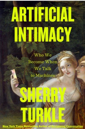
The episode sits in Artificial Intimacy: Who We Become When We Talk to Machines, published by Little, Brown, which runs to 288 pages and sells in the US at $32. It is the fullest statement yet from one of the best-known critics of digital life. Turkle holds the Abby Rockefeller Mauzé chair in the social studies of science and technology at MIT. She trained as a sociologist and as a clinical psychologist. Her view is that heavy chatbot use does harm at every stage of life, from toddlerhood to old age and bereavement.
A career spent on one question
Turkle has been asking what machines do to the people who use them for four decades. The Second Self (1984) and Life on the Screen were early studies of how computers shape identity. Alone Together (2011) looked at social media and social robots, and Reclaiming Conversation (2015) at what phones and texting have done to talk. In 2021 she published a memoir, The Empathy Diaries, which is where the material about her mother comes from.
According to MIT News, she describes her subject as the inner history of technology, meaning not only what a device does but what it does to the person using it. This book applies that approach to chatbots, and it is her most alarmed.
The argument, stage by stage
Unless stated otherwise, Turkle’s remarks and the accounts of the people she interviewed come from material released by MIT. EdPublica did not interview her for this article.
The book is built around the stages of a life, and each section is driven by interviews.
Artificial intimacy, children and attachment
With children, Turkle reports a blurring of categories. One eight-year-old uses the same phone to speak to grandparents and to ChatGPT and files both as things you reach on a phone. A graduate student who uses a chatbot to tell her young daughter bedtime stories says the girl believes there is a person inside the phone. Turkle’s worry is partly about trust, since a device that can state falsehoods without knowing it cannot teach a child what trust is. It is also about solitude. Time alone, she argues, is where children build imagination and a sense of self, and a companion that is always available takes that time away. She calls the stakes for child development existential.
Adults appear as people who started with a practical use and drifted. They include people going through divorce or estrangement who want someone to talk to, students asking for advice on applying to university, and workers who hand assignments to a chatbot. One of her subjects, a middle-aged financial consultant she calls Brian (not his real name), keeps a chatbot with a woman’s name open on a third screen. After a partner ended their relationship, saying he was emotionally unavailable, he put the accusation to the chatbot and asked whether she was right. Turkle’s reading is that he was asking a program with no feelings to rule on feelings.
Her objection is simple to state. A chatbot, she says, produces a performance of empathy. It will tell you it loves you, and it has no stake in whether you hurt yourself or make dinner. People who mistake that performance for the real thing, she argues, begin to find actual people disappointing. Spouses and friends make demands, and the machine only flatters. “We’re starting to define being human as not doing the work,” Turkle said in the MIT material.
On grief, she is blunt. Rebuilding a dead parent or partner as a chatbot, which several people in her book have tried, risks weakening the ability to mourn.
Why people turn to chatbots
Reviewers have noted that Turkle does not treat users as fools. A good part of the book is spent on why the appeal is real. A chatbot gives full attention, never tires, and agrees with you. It spares you the risk of asking someone out or finding the words for a condolence. In her telling, the technology keeps offering to make the harder thing unnecessary, and people keep accepting.
She also admits that some of the demand is a result of a failed supply. Mental health care is hard to reach in the US, and the MIT material says she cites a federal study suggesting only about half of people have access to it. Chatbots are filling the gap, she says, for better or worse. She adds a pointed observation about the industry’s logic: social media thinned out people’s friendships, and chatbots are now sold as the remedy.
The book does not avoid the worst outcomes. Chatbots have been linked to teenagers’ deaths by suicide, in cases that followed long exchanges with chat tools, and Turkle treats these as part of the evidence.
What she wants instead
Her remedy is more cultural than technical. She wants readers to accept that life contains friction and that this is fine. Disagreement, embarrassment and waiting are, in her account, how people learn to cope, and an environment built to remove them leaves people less able to cope. She hopes for a social movement along the lines of the ones against phones in schools and unrestricted social media for the young, and says she would like to be part of it, not alone in it.
She is explicit about her readership. She wanted something that college students and high school seniors could read, and that parents and teachers would not find intimidating. The line she keeps returning to is a question: if the alternative to a richer life in the real world is not clear, what is the point of the exercise?
For the youngest children she is at her most severe. A parent worried that a teenager texts too much is in one kind of conversation, she says. A toddler who thinks a plush toy with a chatbot inside is their best friend is in another, because that touches the foundations of how a person learns to attach. Social media, in her phrase, came for attention, and chatbots come for attachment.
How the book has been received
Publishers’ blurbs have come from Jonathan Haidt, the psychologist behind The Anxious Generation, from former US Surgeon General Vivek Murthy, the author Esther Perel and the philosopher Michael Sandel, among others. Trade reviews have been favourable. Publishers Weekly called it a pointed critique and said it deserved a wide readership, and Kirkus described it as a strong case for resisting the urge to substitute AI for human bonds.
The reservations are of a different kind. Some readers say the book leans on anecdote, and a reviewer for a Christian publication, otherwise admiring, felt a dimension was missing. The method matters here. Turkle is a clinician and an interviewer, and her evidence is case studies and conversations, not controlled trials. That makes the book vivid and persuasive in its details. It also means the question of how common these outcomes are, and whether any chatbot use is benign or helpful, is left largely open. Readers who want the other side of the argument, including from the companies that make these products, will not find it here.


NMC Directs Medical Colleges to Set Up Patient Safety Committees

The Monsoon’s New Rhythm: Less Rain, More Intense Downpours

World Food Day: India’s Childhood Obesity Burden Raises Concerns Over Diabetes Risk

COP17: Can the World Still Meet Its Biodiversity Goals by 2030?

Chandigarh’s Sukhna Wetland Gets Ramsar Recognition, Taking India’s Count to 103

From Scams to Screens: How the National Stock Exchange Rewrote India’s Equity Story

Knowing When to Think for Ourselves: AI, Intuition and the Education of Discernment

After a Scorching Summer, Delhi’s Children Are Slow to Return Outdoors

Two Chemists Win Nobel Prize for Solving a Century-Old Puzzle: Why Life Picks One Hand Over the Other

India’s AI Moment Rests on More Than Code

-

 Math3 months ago
The 2026 Fields Medals: Four Proofs, Four Decades-Old Problems Solved
-
EP Deep Dive: Data & Solutions3 months ago
After Kerala’s Deadliest Landslide, the Hardest Thing to Rebuild Was Childhood
-
EP Deep Dive: Data & Solutions3 months ago
West Asia Crisis: Can Kerala’s Returning Gulf Migrants Find a Future in the Green Economy?
-
Space & Physics5 months ago
India Semiconductor Mission: ‘It’s Not About Fabs. It’s About Building An Entire Ecosystem’
-
Interviews3 weeks ago
From Scams to Screens: How the National Stock Exchange Rewrote India’s Equity Story
-
Climate5 months ago
The Climate World Cup? How Climate Change Could Affect Player Performance at the 2026 World Cup
-
Society3 months ago
What Is Civilisational Diplomacy? Understanding India’s Newest Foreign Policy Tool
-
Society4 months ago
From Bell Labs to the Classroom: A Second Career in Teaching