Space & Physics
Why Jupiter Has Eight Polar Storms — and Saturn Only One: MIT Study Offers New Clues
Two giant planets, made of the same elements, display radically different storms at their poles. New research from MIT now suggests that the key to this cosmic mystery lies not in the skies, but deep inside Jupiter and Saturn themselves.

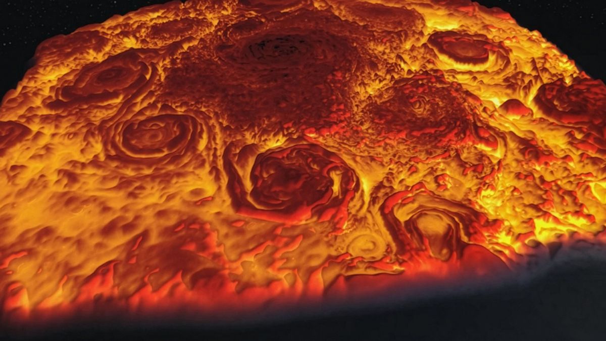
For decades, spacecraft images of Jupiter and Saturn have puzzled planetary scientists. Despite being similar in size and composition, the two gas giants display dramatically different weather systems at their poles. Jupiter hosts a striking formation: a central polar vortex encircled by eight massive storms, resembling a rotating crown. Saturn, by contrast, is capped by a single enormous cyclone, shaped like a near-perfect hexagon.
Now, researchers at the Massachusetts Institute of Technology believe they have identified a key reason behind this cosmic contrast — and the answer may lie deep beneath the planets’ cloud tops.
In a new study published in the Proceedings of the National Academy of Sciences, the MIT team suggests that the structure of a planet’s interior — specifically, how “soft” or “hard” the base of a vortex is — determines whether polar storms merge into one giant system or remain as multiple smaller vortices.
“Our study shows that, depending on the interior properties and the softness of the bottom of the vortex, this will influence the kind of fluid pattern you observe at the surface,” says study author Wanying Kang, assistant professor in MIT’s Department of Earth, Atmospheric and Planetary Sciences (EAPS) in a media release issued by the institute. “I don’t think anyone’s made this connection between the surface fluid pattern and the interior properties of these planets. One possible scenario could be that Saturn has a harder bottom than Jupiter.”
A long-standing planetary mystery
The contrast has been visible for years thanks to two landmark NASA missions. The Juno spacecraft, which has been orbiting Jupiter since 2016, revealed a dramatic polar arrangement of swirling storms, each roughly 3,000 miles wide — nearly half the diameter of Earth. Cassini, which orbited Saturn for 13 years before its mission ended in 2017, documented the planet’s iconic hexagonal polar vortex, stretching nearly 18,000 miles across.
“People have spent a lot of time deciphering the differences between Jupiter and Saturn,” says Jiaru Shi, the study’s first author and an MIT graduate student. “The planets are about the same size and are both made mostly of hydrogen and helium. It’s unclear why their polar vortices are so different.”
Simulating storms on gas giants
To tackle the question, the researchers turned to computer simulations. They created a two-dimensional model of atmospheric flow designed to mimic how storms might evolve on a rapidly rotating gas giant.
While real planetary vortices are three-dimensional, the team argued that Jupiter’s and Saturn’s fast spin simplifies the physics. “In a fast-rotating system, fluid motion tends to be uniform along the rotating axis,” Kang explains. “So, we were motivated by this idea that we can reduce a 3D dynamical problem to a 2D problem because the fluid pattern does not change in 3D. This makes the problem hundreds of times faster and cheaper to simulate and study.”
The model allowed the scientists to test thousands of possible planetary conditions, varying factors such as rotation rate, internal heating, planet size and — crucially — the density of material beneath the vortices. Each simulation began with random chaotic motion and tracked how storms evolved over time.
The outcomes consistently fell into two categories: either the system developed one dominant polar vortex, like Saturn, or several coexisting vortices, like Jupiter.
The decisive factor turned out to be how much a vortex could grow before being constrained by the properties of the layers beneath it.
When the lower layers were made of softer, lighter material, individual vortices could not expand indefinitely. Instead, they stabilized at smaller sizes, allowing multiple storms to coexist at the pole. This matches what scientists observe on Jupiter.
But when the simulated vortex base was denser and more rigid, vortices were able to grow larger and eventually merge. The end result was a single, planet-scale storm — remarkably similar to Saturn’s massive polar cyclone.
“This equation has been used in many contexts, including to model midlatitude cyclones on Earth,” Kang says. “We adapted the equation to the polar regions of Jupiter and Saturn.”
The findings suggest that Saturn’s interior may contain heavier elements or more condensed material than Jupiter’s, giving its atmospheric vortices a firmer foundation to build upon.
“What we see from the surface, the fluid pattern on Jupiter and Saturn, may tell us something about the interior, like how soft the bottom is,” Shi says. “And that is important because maybe beneath Saturn’s surface, the interior is more metal-enriched and has more condensable material which allows it to provide stronger stratification than Jupiter. This would add to our understanding of these gas giants.”
Reading the interiors from the skies
Planetary scientists have long struggled to infer the internal structures of gas giants, where pressures and temperatures are far beyond what can be reproduced in laboratories. This new work offers a rare bridge between visible atmospheric patterns and hidden planetary composition.
Beyond explaining two of the Solar System’s most visually striking storms, the research could shape how scientists interpret observations of distant exoplanets as well — worlds where atmospheric patterns might be the only clues to what lies within.
For now, Jupiter’s swirling crown of storms and Saturn’s solitary hexagon may be doing more than decorating the poles of two distant giants. They may be quietly revealing the deep, unseen architecture of the planets themselves.






Space & Physics
NASA Puts $500,000 Prize on Better Satellite Tracking
NASA is offering up to 500,000 dollars to develop affordable technology that can improve satellite tracking by measuring atmospheric drag in low Earth orbit. The effort aims to help operators predict orbital changes more accurately as solar activity alters the thin upper atmosphere.
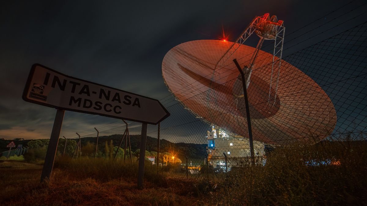
A faint layer of air high above Earth is becoming an important concern for satellite tracking operators. NASA is now offering up to USD 500,000 to individual winning teams that can develop a practical way to monitor it. The US space agency opened the Orbital Clarity Challenge on August 19, asking researchers and companies to develop instruments that can determine how much drag spacecraft experience in low Earth orbit. Up to four teams can win the top prize, taking the potential total award to USD 2 million.
The focus is the thermosphere, a region that begins about 80 kilometres above Earth and extends hundreds of kilometres into space. The air here is extremely sparse, but spacecraft moving through it still encounter enough resistance to gradually alter their orbits.
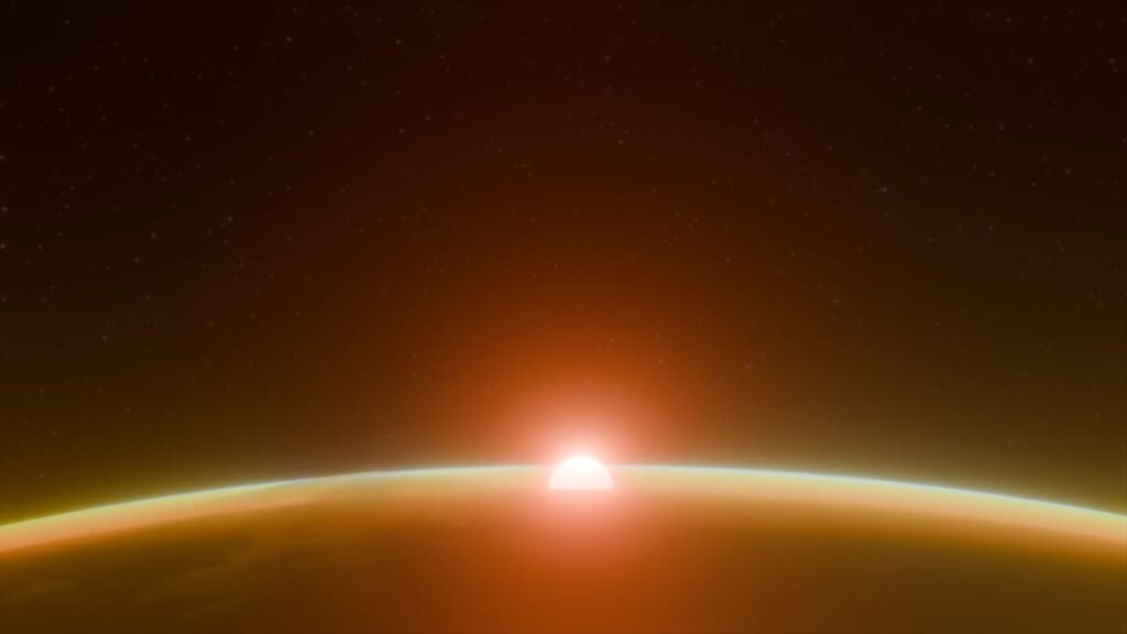
That resistance does not remain constant. When the Sun becomes more active, bursts of energy can heat the upper atmosphere. The thermosphere expands, increasing the amount of gas encountered by satellites. The resulting increase in drag can change their altitude and make their future position harder to calculate. For spacecraft operators, even a small difference can matter when several objects are moving through the same orbital region.
A Gap in the Data
NASA already relies on computer models to estimate atmospheric drag. But those calculations depend on how well scientists understand conditions in the upper atmosphere at a particular time and location. The agency wants new technology that can provide more direct information.
Under the competition, proposed instruments should be inexpensive enough to be deployed widely. NASA says they could potentially be carried aboard commercial spacecraft as hosted payloads, allowing measurements to be collected from several points in orbit rather than from a limited number of dedicated missions.
The competition will run through several stages, with NASA aiming to move successful ideas from an initial concept towards an instrument that can eventually be tested in space. Winning teams are also expected to receive an opportunity for an orbital demonstration. Applications for the first stage close in November 2026.
Satellite Tracking: Why this Matters?
The number of spacecraft operating in low Earth orbit has grown rapidly, with satellites supporting communications, navigation, Earth observation and scientific research.
Their paths are affected by several forces, including the thin atmosphere at orbital altitude. During periods of strong solar activity, atmospheric drag can rise sharply and contribute to changes in orbital altitude. Better information about those changes could help operators plan manoeuvres more accurately and improve forecasts of when satellites will descend from orbit.
NASA’s prize is therefore aimed at a relatively small piece of the space infrastructure puzzle: getting a clearer picture of the air that satellites are still moving through, even hundreds of kilometres above the ground.
Space & Physics
Sophie Adenot Makes History as First Frenchwoman to Walk in Space
French astronaut Sophie Adenot has become the first Frenchwoman to perform a spacewalk, spending 6 hours 23 minutes outside the International Space Station.

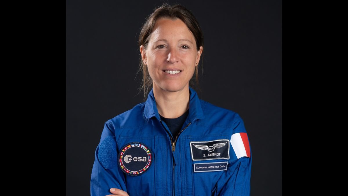
French astronaut Sophie Adenot has become the first Frenchwoman to perform a spacewalk, spending 6 hours and 23 minutes outside the International Space Station to begin repairs to its exterior communications system.
French astronaut Sophie Adenot made European space history on Tuesday by becoming the first French woman to perform a spacewalk outside the International Space Station. Adenot, 44, stepped outside the orbiting laboratory alongside American astronaut Anil Menon, floating roughly 400 kilometres above the Earth for 6 hours and 23 minutes to begin a repair of the station’s exterior communications equipment.
“I’m out,” Adenot said as she exited the station. “I feel very good now.”
A Repair Job That Ran Long The astronauts’ task was to replace an aging space-to-ground antenna on the station’s Z1 truss — the primary link carrying high-speed data, voice calls and video between the station and mission control in Houston. The antenna had stopped tracking NASA’s data relay satellites since November and had been out of service since, with a second antenna carrying the station’s communications load in the meantime.
Menon and Adenot successfully removed the failed antenna and secured it to the truss structure, but disconnecting its electrical cables and loosening its mounting bolts took longer than planned, leaving no time to install the replacement unit. NASA has scheduled a second spacewalk for Tuesday, August 25, to complete the installation. The station’s communications were not affected by the delay, as the backup antenna continued operating throughout.
Inside the station, astronauts Jack Hathaway and Jessica Meir coordinated the operation from the control desk, operating the station’s robotic arm and monitoring the spacewalkers’ life support systems throughout.
Days of Preparation Before the Hatch Opened Spacewalks demand days of preparation before the airlock ever opens. In the lead-up, Adenot and Menon spent dozens of hours readying their gear inside the station — inspecting safety tethers, organising tools, servicing backup emergency jetpacks, charging suit batteries, checking for pressure leaks, and testing biomedical sensors and radios.
Spacewalk complete. ✅
After 6 hours and 23 minutes outside the International Space Station, @Soph_astro is safely back inside.
With today’s EVA, Sophie becomes the first French woman to perform a spacewalk. 🇫🇷 pic.twitter.com/i3BghrdaRK— European Space Agency (@esa) August 18, 2026
“A successful [spacewalk] starts long before the hatch opens, and that’s where my focus has been these past few days: rehearsing, preparing and focusing,” Adenot said on social media before the excursion.
Suit fitting was a major focus of the preparation: working inside a heavy, pressurised spacesuit for over six hours puts considerable strain on an astronaut’s hands and shoulders, and engineers on the ground worked closely with Adenot to customise her suit and reduce pressure points.
A Milestone for European Space Exploration Adenot brought extensive technical experience to the mission. A trained engineer and former helicopter test pilot, she was selected for astronaut training by the European Space Agency in 2022 and launched to the space station in February 2026, becoming only the second French woman in history to reach space, after physician-astronaut Claudie Haigneré in 1996. With Tuesday’s spacewalk, she also became the second European woman ever to conduct a spacewalk, after Italian astronaut Samantha Cristoforetti in 2022, and the fifth French citizen overall to do so. The last French citizen to walk in space was Thomas Pesquet.
Despite the milestone, Adenot credited the wider team behind the mission. “My deepest gratitude goes to everyone who made this possible — pioneers who came before us, but also the incredible teams working behind the scenes today,” she said after returning inside the station.
Space & Physics
Hubble and Gaia Uncover Evidence of Ancient Dwarf Galaxy Devoured by the Early Milky Way
Hubble and Gaia reveal evidence of an ancient Milky Way merger with a dwarf galaxy about 11.8 billion years ago, reshaping our understanding of the galaxy’s origins.
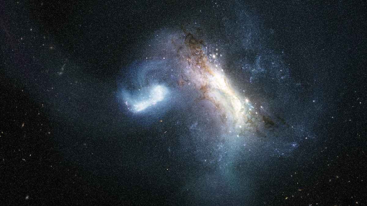
A Milky Way merger with a dwarf galaxy about 11.8 billion years ago has been uncovered by astronomers using the Hubble Space Telescope and ESA’s Gaia mission. The discovery provides new evidence about how the Milky Way formed and identifies a distinct population of ancient globular clusters linked to the merger.
Our home galaxy, the Milky Way, contains hundreds of billions of stars today. It grew to this size over billions of years by pulling in smaller neighbouring galaxies and absorbing them. Now, astronomers using the NASA/ESA Hubble Space Telescope and ESA’s Gaia mission have found evidence of a major merger that occurred near the very beginning of the Milky Way’s history.
By combining precise stellar age and chemical-composition measurements from Hubble with motion-mapping data from Gaia, the team pushed back the known timeline of the Milky Way’s formation by roughly 1.8 billion years. The findings, led by Davide Massari of the Astrophysics and Space Science Observatory of Bologna, Italy, were published this week in Nature Astronomy.
Evidence of an Ancient Milky Way Merger
Reconstructing the Milky Way’s earliest history is difficult: in its youth, the galaxy was smaller, more chaotic, and closer in size to the dwarf galaxies it collided with, and many physical traces of those early mergers have since been erased.
To work around this, the researchers studied 39 globular clusters — dense, ancient groupings of up to a few million stars — in the inner 20,000 light-years of the galaxy, where evidence of the earliest mergers is most likely to survive. Using Hubble’s high-resolution imaging, the team measured each cluster’s age and metallicity (its abundance of elements heavier than helium) with what the researchers describe as unprecedented precision.
“Thanks to the high resolution and depth of Hubble imaging, we could measure the age and the metal content of these clusters with unprecedented precision,” said Chiara Zerbinati, a co-author on the study at the University of Bologna, in a release issued by ESA Hubble. “Coupled with measurements from Gaia, this made it possible to distinguish a population of globular clusters that are different from the others.”
Identifying LKH
Cross-referencing Hubble’s age and metallicity data with Gaia’s motion measurements, the researchers identified a distinct third population of globular clusters — older than the ones known to have arrived during the Milky Way’s collision with the Gaia-Sausage-Enceladus dwarf galaxy about 10 billion years ago, but younger than the stars that formed within the Milky Way itself.
That pattern pointed to a separate, earlier merger: the absorption of a dwarf galaxy roughly 11.8 billion years ago — about two billion years after the Big Bang — carrying a total stellar mass of around 500 million times the mass of the Sun, a significant share of the Milky Way’s total mass at the time.
The researchers named the dwarf galaxy Low-energy-Kraken-Heracles, or LKH, after three earlier papers that had proposed the idea of an early merger in the Milky Way’s history.
“Our home is the Milky Way galaxy, but we do not know how our house was built,” Massari said. “In this paper we discover where the first significant batch of bricks came from: a dwarf galaxy that we call LKH.”
Rewriting Early Galactic History
The finding challenges an earlier assumption that the Milky Way’s oldest stellar populations formed almost entirely in place, showing instead that external galaxies contributed to its structure far earlier than previously established.
The team plans to extend the analysis to additional globular clusters across the galaxy, aiming to build a more complete map of the mergers that shaped the Milky Way over cosmic history.


Chinese Humanoid Robots Beat Human Records at Beijing Games

Our Algorithm Knows What We Want Before We Do. That is the Problem.

Scientists Map Earth’s Sand Dunes in a New Global Survey

NASA Puts $500,000 Prize on Better Satellite Tracking

Why India Is Studying the Arctic to Understand Its Monsoon

After Kerala’s Deadliest Landslide, the Hardest Thing to Rebuild Was Childhood

When the Monsoon Returns, Fear Returns: How Climate Disasters Are Reshaping Mental Health in Himachal Pradesh

Astronomers Discover a ‘Black Hole Star’, a New Kind of Object in the Early Universe

From Bell Labs to the Classroom: Finding Purpose After Retirement

Why Is India Flooding If El Niño Predicted a Weak Monsoon?
-

 Math1 month ago
The 2026 Fields Medals: Four Proofs, Four Decades-Old Problems Solved
-
Climate4 weeks ago
After Kerala’s Deadliest Landslide, the Hardest Thing to Rebuild Was Childhood
-
Society2 months ago
West Asia Crisis: Can Kerala’s Returning Gulf Migrants Find a Future in the Green Economy?
-
Space & Physics3 months ago
India Semiconductor Mission: ‘It’s Not About Fabs. It’s About Building An Entire Ecosystem’
-
Climate3 months ago
The Climate World Cup? How Climate Change Could Affect Player Performance at the 2026 World Cup
-
Society1 month ago
What Is Civilisational Diplomacy? Understanding India’s Newest Foreign Policy Tool
-
Society2 months ago
From Bell Labs to the Classroom: A Second Career in Teaching
-
Space & Physics3 months ago
Engineers Develop Dual-Mode Propulsion System for Next-Generation Small Satellites