Society
Study what you love, to love what you do
“It’s OK to take time, and not want to be a part of the rat race,” says Sai Shruti, a physics and history of science graduate, about pursuing educational goals. EdPublica interviewed Sai Shruti for the International Day for Women and Girls in STEM 2024.


On the occasion of the International Day for Women and Girls in Science this year, EdPublica set out to interview ambitious young women from across the world, exploring their interests in science and beyond.
EdPublica‘s science editor Karthik Vinod interviewed Sai Shruti Sudarsan, a physics and history graduate who’s into content creation and Carnatic music from India.
Sai Shruti recently completed her master’s degree in history and philosophy of science from the prestigious University College London (UCL) in the UK. Before this, she did her bachelor’s honors degree in physics from the Sri Sathya Sai Institute of Higher Learning in India. Now back in India, she’s doing a correspondence degree in Carnatic Music from the University of Madras.
We asked Sai Shruti about her academic journey so far, her aspirations, and whether she could lend a piece of advice to our young readers, about pursuing educational goals.
The e-mail interview between Sai and Karthik was edited for brevity. Here are the excerpts:
Hello Sai, thanks for agreeing to be interviewed!
You’ve returned from the UK having done your master’s studies just now. And previously, you’d done your undergraduate studies in India. How would you compare your academic experience in India with the UK?
I had extremely contrasting experiences but I’m very happy I got to undergo both of them. College in the UK was very flexible and I had to do a lot of self-studying and had to take full responsibility of my own learning. I was free to explore my interests in the field and had many modules to choose from. College in India felt like an extended version of schooling—we were made to study and work so independent learning was less, but I think at a bachelor’s level I needed the hand-holding I got.
How did you manage your life in the UK – between balancing academics with socializing, and taking up personal responsibilities? What was your day like?
If this was a video or in-person interview, you would’ve seen me laughing! Being the introvert I was (I’ve become a bit more social now), I didn’t have much of a social life. Personal responsibilities were just household work which I was able to manage pretty well. I was a part-time tutor at a tuition center which took about 10 hours of my week. Apart from that I had ample time to focus on music and I found myself creating a lot of stuff there. Academics were chill—my course did not demand as much time as a proper STEM course would, so I had time for everything.
Did you have any ‘culture shocks’ upon arriving for the first time in the UK?
Although I expected to receive some, I got none really. I found it comfortable and adapted very quickly. Maybe the only shock I had was when looking at those price tags :’) I had to train myself to stop converting pounds to rupees when buying my necessities.
What interested you to pursue physics? What did you aspire to become?
I’d give all the credits to my physics tuition teacher in my 11th & 12th grade for that.
I opted for the science stream after 10th grade, because the commerce stream seemed more alien to me, and arts weren’t an option back then. Going for tuitions was (and still seems to be) the norm, but neither my parents nor I was keen to join one at first. I joined tuitions for physics because someone had recommended my teacher to me – and that was and still is – one of the best decisions I’d made in my life so far (so much so that my teacher occupied quite some space in my SOP for master’s)! He made me fall in love with not just physics, but with science and learning in general.
But here’s the thing—I still don’t have any great aspirations to become a “scientist”, or anything ‘big’ in STEM after 12th grade. I was always into the arts, especially music. But having a BSc. Physics degree seemed safer and more practical than having a bachelor’s in music. I can pursue music any time – in fact, I’m doing that right now. So, my bachelor’s in physics happened, and I didn’t go into core STEM after that. And I didn’t 😉
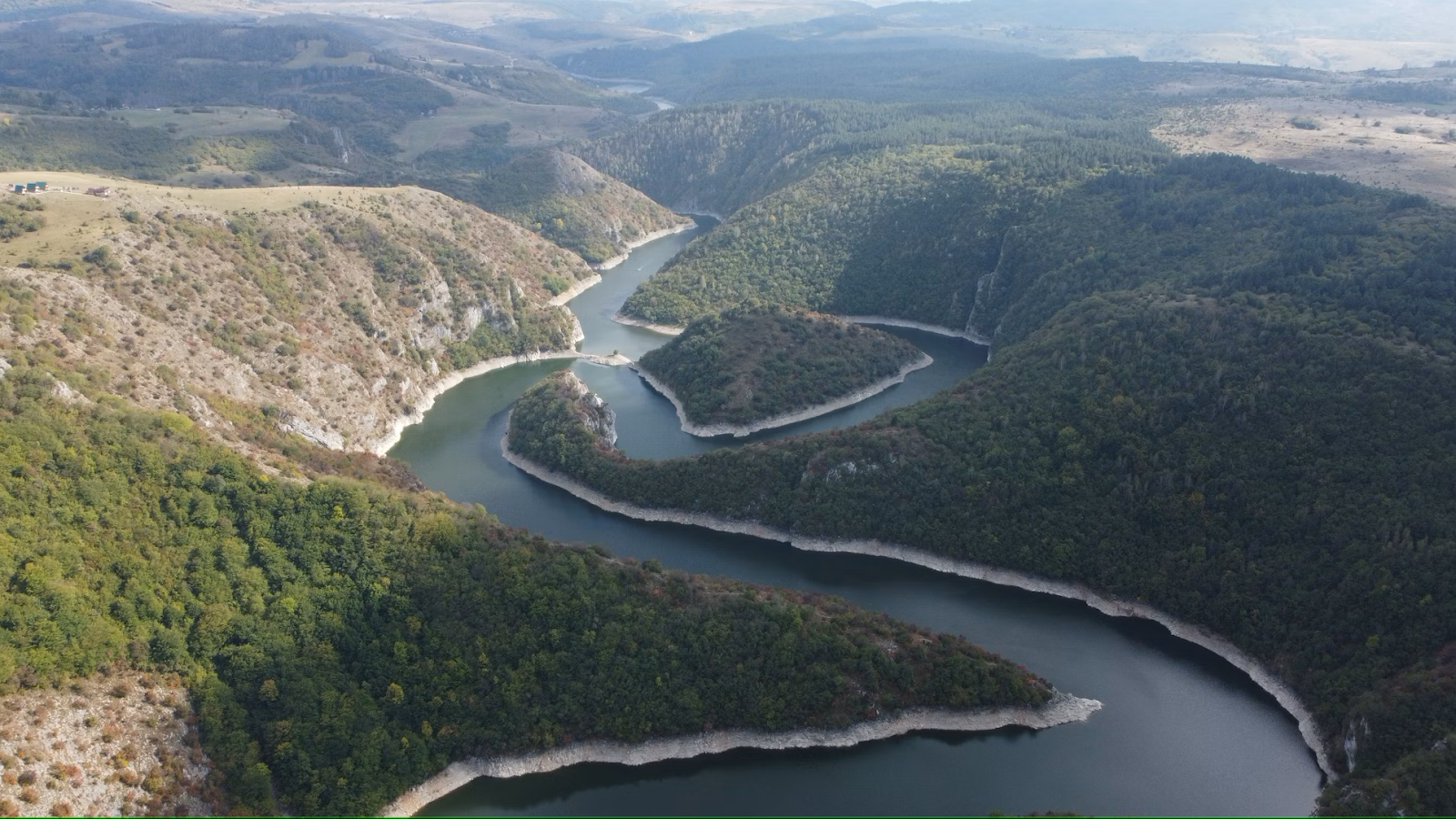
“Go with the flow”, Courtesy: Anton Lukin / Unsplash
And what has changed for you since then, to do a master’s in history and philosophy of science in the UK? How has that added value to you and your career prospects?
I stood by my decision to not get into core STEM, but I wanted to stay in touch with science, especially physics.
After my bachelor’s degree, I took a break to research possible courses, and ended up discovering history and philosophy of science. I went through some online courses to understand what it was all about, and whether I’d really like doing it, ultimately landing at UCL to do my MSc. History and Philosophy of Science.
I found myself liking history of science and science communication more, which then opened me up to do public engagement and science journalism. That’s the career path I’m embarking on right now.
Did you face any resistance from your family for pursuing your interests?
I’m ever grateful, and feel extremely lucky for my parents’ unwavering support in whatever I’ve done until now. I faced absolutely no resistance from them about pursuing my niche interests. In fact, I actually got more support and understanding from them! I’ve had the complete freedom to explore my passion and interests in order to do what I truly love.
That’s nice to hear! So, what are you doing currently?
I work at Previu, an AI-driven healthcare startup which focuses on lifestyle transformation and cancer care. I hold an official designation there as “Scientific Content Writer”, but I mostly manage social media and content.
Not so much writing, but I create content in addition to designing brochures, templates, flyers and such for the company. So I’d say I’m in the marketing and branding department of the company, playing a role in the digital side of things.
So, what’s next for you now – as in your future goals?
I had a lot of potential research questions while doing my MSc at UCL , which I would love to work on. So, my future goal would be to do a PhD in history of science. I see a future in education … I love teaching!
How do you feel about there being an International Day for Women and Girls in STEM this Sunday?
I wasn’t aware of this until you brought this up! But I think it’s a good initiative to acknowledge, encourage and appreciate the minority of women there is in STEM. Science, or more generally, knowledge, should never be a gender thing! It’s good to see more platforms and initiatives breaking such stereotypes.
That’s great! What would you like to tell girls and boys – or their parents – about making choices about college education? How did you ultimately choose your path and remain committed?
Take your time. But RESEARCH! Talk to people and get their perspectives. But keep in mind that the final decision must still be yours! It’s crucial to study what you love, in order to love what you do. It’s OK to take time, and not want to be a part of the rat race.
Circumstances definitely differ. Many may not have the time or space to do things at their pace. For financial difficulties contribute majorly to what and where you do it. But you’re not alone in this world. There are people ready to guide and help, so never hesitate to ask.
I’m a literal “go with the flow” kind of person. I’m not being pretentious or trying to be cool here. It’s not a great attitude for someone with ambitious goals. But I think it’s OK, since I’m in a relatively better mental and financial space to let myself not be anxious and actively plan my future.
All credits to my parents for providing me with the liberty, and keeping me in that position! So I don’t have much advice for being focused on goals—I still don’t know what, or where I would be in the next two years. I do have a destination in mind, but I absolutely have no idea about the path I’m going to take. We’ll figure that out along the way 😉








Society
India’s Investment Growth Has Doubled. Is Private Capital Finally Moving?
India’s investment growth is accelerating, with GFCF rising 11.9% in Q1 FY27. But the bigger question is whether this momentum signals a sustained revival in private capital. From factory utilisation and bank credit to manufacturing and employment, the next few quarters will reveal whether India’s public investment push is finally drawing private businesses into a broader investment cycle.

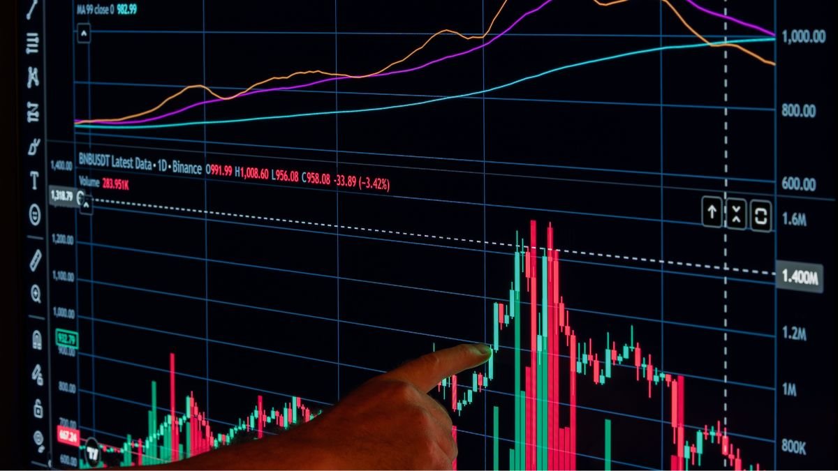
India’s latest GDP numbers offer a reason to look beyond the headline 7.8% growth. Gross fixed capital formation (GFCF), a measure of private investment in fixed assets across the economy, grew 11.9% in the first quarter of 2026-27, compared with 5.8% a year earlier. Its share of nominal GDP also increased to 34.3%, from 31.4% a year earlier.
Other indicators point in the same direction. Capital-goods production grew 15.2% in the quarter, compared with 8.8% a year earlier, while industrial credit expanded 20% year-on-year in July, compared with 6.5% a year earlier.
The numbers suggest that investment activity is gaining momentum. But raising concern is whether India is finally moving from a period of government-led capital spending towards a broader private investment cycle?
From Public Capex to Private Investment
For several years, public capital expenditure has been central to India’s growth strategy. The government has invested heavily in roads, railways, ports, power and other infrastructure, with the broader objective of improving connectivity and lowering the cost of doing business.
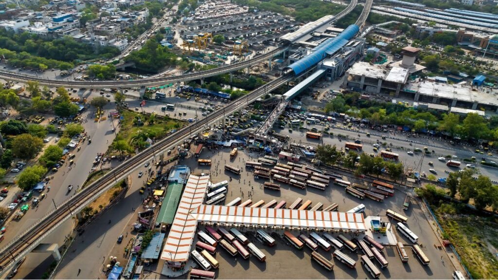
The idea was not simply for the government to build more infrastructure. Public investment was also expected to create conditions in which businesses would become more willing to invest in factories, machinery and new capacity. The latest data provide some evidence that this process may be gaining traction.
GFCF grew 11.9% in Q1 FY27, more than twice the 5.8% growth recorded a year earlier. Capital-goods production also accelerated, growing 15.2% in the quarter. In July, capital-goods production increased another 16.1%. Industrial credit provides another signal. Lending to industry grew 20% year-on-year in July, compared with 6.5% a year earlier.
Taken together, these indicators suggest that the investment story is broader than a single GDP component. But they do not, by themselves, prove that India has entered a private investment boom. GFCF measures investment across the economy; it is not the same as private capital expenditure.
Is Private Capital Actually Returning?
This is the more important test. Reuters reported that private-sector capital investment increased by more than 5 trillion rupees from a year earlier during the April-June quarter. It pointed to stronger factory utilisation, healthier corporate balance sheets and rising bank credit as some of the factors supporting the revival.
There is another encouraging signal from the Centre for Monitoring Indian Economy (CMIE). Private companies announced projects worth 15.4 rupees lakh crore during the quarter, a 97% increase from a year earlier. But project announcements are not the same as money actually being spent. Companies can delay, scale down or abandon projects after announcing them.
That distinction matters because private capital expenditure had actually moderated in FY26. A Union Bank of India analysis reported by The Tribune found that private capex fell 2.8% to 11.9 lakh crore rupees in FY26 from 12.3 lakh crore rupees in FY25, after reaching a record level the previous year. The picture, therefore, is not of a private investment boom that has already been established. It is a possible revival that still needs to prove itself.
Why Might Companies be Investing Now?
One possible explanation is that existing industrial capacity is being used more intensively. When factories operate closer to capacity, companies have less room to increase output using existing machinery. That can make investment in new equipment, facilities and production lines more attractive.
Recent Reserve Bank of India assessments indicate that capacity utilisation has moved above its long-term average. Reuters reported that factory utilisation approached 77% in the fourth quarter of FY26. At the same time, corporate balance sheets have strengthened and bank credit has accelerated.
These conditions can reinforce each other. Higher utilisation can encourage investment. New investment can increase production capacity. Stronger demand can then encourage another round of expansion. But this cycle depends on one thing: whether companies believe demand will remain strong enough to justify investing in new capacity.
Where is the Money Going?
The sectoral composition provides another clue. Manufacturing grew 9.2% in Q1 FY27. Within manufacturing, electrical equipment production increased 27%, other transport equipment 19.5%, and computer, electronic and optical products 12.4%. These are among the sectors central to India’s effort to expand domestic manufacturing and build strategic industrial capacity.
Government policy is reinforcing this direction. The Mobile Phone Manufacturing Scheme, approved in July, has an outlay of 62,500 crore rupees through 2030-31. Semicon 2.0 has an allocation of 1.275 lakh crore rupees for areas including chip design, manufacturing, advanced packaging and research. These are government outlays designed in part to catalyse private investment. They should therefore not be treated as private capital expenditure themselves.
The bigger question is whether such support helps create industries that can eventually compete and expand without remaining permanently dependent on government incentives.
The Employment Test
More investment means more factories, machinery and infrastructure. But it does not automatically mean more jobs. The employment impact depends heavily on what is being built. A highly automated semiconductor facility can involve enormous capital expenditure while creating relatively few direct jobs compared with a labour-intensive manufacturing plant.
For India, this distinction matters. A successful investment cycle should ideally do more than increase the value of fixed assets. It should raise production, improve productivity and create employment, particularly in sectors capable of absorbing large numbers of workers.
The current GDP data cannot yet tell us whether that is happening. That makes employment one of the most important tests of the investment revival in the quarters ahead.
The Demand Problem
There is another basic question: who will buy what the new investment produces? Household consumption grew 7.1% in Q1, while exports grew 12%. Both provide some support for companies considering expansion.
But investment decisions depend on expectations about future demand, not just one quarter’s performance. If domestic consumption weakens, businesses may postpone capacity expansion. If global trade becomes more uncertain, export-oriented companies could face the same pressure.
India is therefore attempting to build a private investment cycle while the global economy remains exposed to geopolitical tensions and trade uncertainty. That makes the transition from public investment to private investment more difficult than simply recording one strong quarter.
The Real Test Begins Now
The 11.9% increase in GFCF matters because it is accompanied by several other positive signals. Capital-goods production is rising. Industrial credit has accelerated. Manufacturing is expanding. Private companies are announcing more projects. Corporate capacity utilisation has strengthened.
But one quarter cannot establish a structural investment cycle. The more meaningful test will be whether companies continue to announce and execute new projects over the next several quarters; whether investment spreads beyond a limited group of sectors; and whether higher capital formation translates into greater production and employment.
The investment numbers also need to be read alongside the broader debate over India’s revised GDP methodology. The government has defended the new series, while some economists have raised questions about aspects of the estimates. That debate makes it even more important to look at several independent indicators rather than relying on the GDP figure alone.
For now, the data offer something more useful than a declaration of an investment boom. They suggest that the conditions for a shift from public investment towards stronger private capital formation may be improving. Whether that becomes a durable engine of India’s growth will depend less on what happened in one quarter than on what businesses do next.
Society
Farmers Borrowed to Build ‘Diggis’. Two Years Later, They Are Still Waiting for the Subsidy
Farmers in Rajasthan’s Hanumangarh district built diggis, farm ponds and other water structures after receiving government approval under the Atal Bhujal Yojana. But with crores in subsidies pending, many say they are now left paying loans and waiting for the money they were promised.

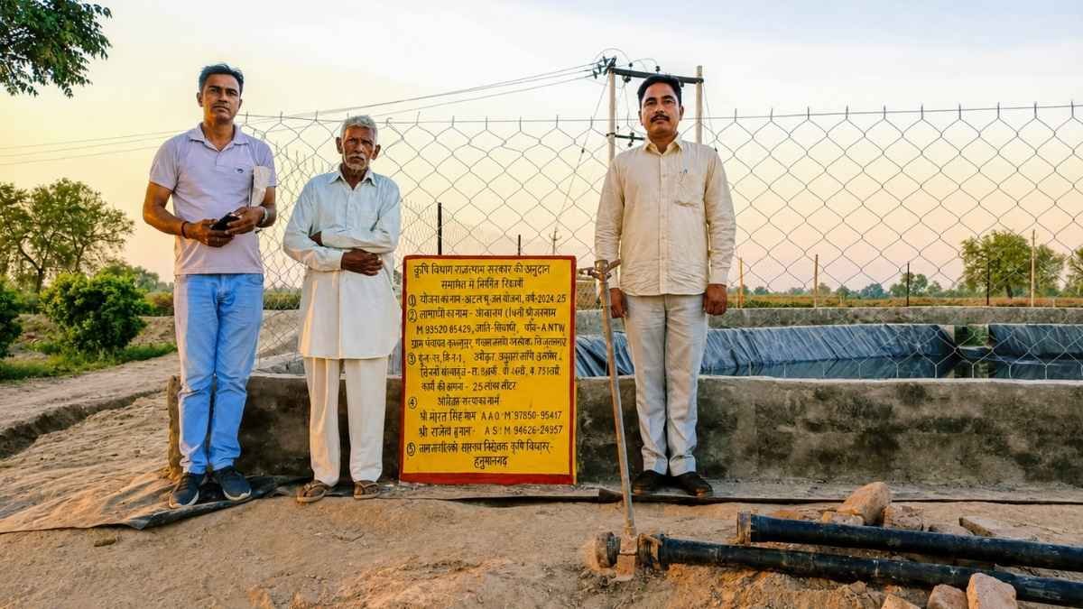
Farmers in Rajasthan’s Hanumangarh district built diggis and other water structures after receiving government approval. But with the Atal Bhujal Yojana subsidy still pending, many are left paying loans and waiting for the money they were promised.
Rajaram Bishnoi, a farmer from Chak 4 NTW in Bhagatpura gram panchayat (village council area) of Rajasthan’s Hanumangarh district, applied to the Agriculture Department in 2024-25 under the Atal Bhujal Yojana (Atal Groundwater Scheme) to build a water diggi [a small farm reservoir dug into the ground to store rainwater and canal water for irrigation] with a capacity of 25 lakh litres on his farm. He was in the general category of farmers. The department approved his application. Rajaram then built the diggi on his farm. It cost him around Rs 5 lakh, but he is still waiting for the subsidy from the government.
Rajaram says that the government considers the cost of a diggi to be Rs 4 lakh and gives 75 per cent of this amount as subsidy to farmers in the general category. But the actual cost is higher. He said, “When I built the diggi on my farm, it cost around Rs 5 lakh. I was satisfied thinking that the government would at least give Rs 3 lakh as subsidy. But even after around two years, we have not received the subsidy amount.”
His son, Sushil Kumar Bishnoi, says they borrowed money from a commission agent at an interest rate of Rs 2 per hundred (i.e., 2 per cent, commonly charged per month in informal rural lending) and used it to build the diggi. “We thought that we would soon get the money from the government and repay the loan. But so far, all we have got is the wait. We have to pay the interest every month.”
Atal Bhujal Yojana Subsidy Leaves Rajasthan Farmers Waiting
Rajaram Bishnoi is not the only farmer waiting for the subsidy after building a diggi. Thousands of farmers in Rajasthan built diggis, farm ponds and water structures such as pipelines under the government scheme to save groundwater and increase the availability of water on their farms. They made this investment after getting government approval and in the hope of receiving the subsidy. But now, in Hanumangarh district, subsidy amounting to Rs 38 crore 52 lakh 6 thousand for the work done in two financial years is pending, and farmers have been protesting for a long time to get the money.
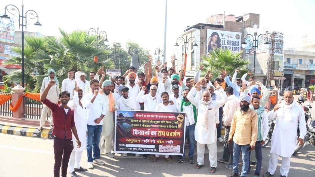
According to official figures from Hanumangarh district, farmers built 829 diggis, four farm ponds, purchased six agricultural machines, and laid 10 pipelines in 2024-25. A subsidy of Rs 25 crore 15 lakh 73 thousand is pending for these works. In 2025-26, 410 diggis, 12 farm ponds, 64 agricultural machines, and 40 pipelines were completed, and mini kits [small government-supplied packages of seeds, tools, or inputs] were also distributed. Payments of more than Rs 13.36 crore for these works are pending.
Crucially, many farmers in 2025-26 carried out the construction after getting approval from the government. But after the Atal Bhujal Yojana ended in October 2025, instructions were issued to stop the work. Resham Singh Manuka, district president of the Bharatiya Kisan Union [Indian Farmers’ Union, a national farmers’ advocacy organisation], asks, “When a farmer has invested money on his own land on the basis of government approval and has completed the construction, why is the financial risk of the scheme ending later being passed on to the farmer?”
This question is also important because the central government implemented the Atal Bhujal Yojana from April 1, 2020 to October 15, 2025 in 8,203 water-stressed gram panchayats in 229 blocks of 80 districts across seven states — Gujarat, Haryana, Karnataka, Madhya Pradesh, Maharashtra, Rajasthan and Uttar Pradesh. It was a pilot scheme for a fixed period. On July 30, 2026, Union Minister of State for Jal Shakti [India’s federal ministry overseeing water resources, river development, and drinking-water supply] Raj Bhushan Choudhary, in a written reply to a question in the Lok Sabha [the lower house of India’s Parliament], said the impact of the scheme was positive. He said that according to the 2023-25 assessment, improvement in groundwater levels was seen in 180 out of 229 blocks.
The government’s own assessment credits the scheme with improving groundwater levels in 180 of the 229 blocks it covered. But whether that technical success reaches farmers depends on the government actually paying what it approved — and in Hanumangarh, that payment is where the scheme is failing.
There is also a long chain of farmers’ protests and government assurances over the payment of the subsidy. On March 6, 2026, after farmers surrounded the office of the Joint Director of Agriculture in Hanumangarh, a written agreement was reached between officials and farmer representatives. It assured that the pending diggi subsidy for 2024-25 would be paid within two months. When the payment did not happen, farmers surrounded the district collectorate and Agriculture Office on May 19. They were then assured that the payment would be made within one month and 15 days. The issue was also raised in the district-level review meeting on June 22. When C.R. Chaudhary, chairman of the State Farmers Commission, visited Hanumangarh on July 30, farmers raised the issue before him.
He told farmers that the subsidy was pending not only for farmers in Hanumangarh but across the state. “I had a courtesy meeting with Union Jal Shakti Minister C.R. Patil in New Delhi and held detailed discussions on important issues related to the interests of farmers in Rajasthan,” Chaudhary said. He said he had written to the Union Minister requesting early payment of the pending subsidy amount for 38 blocks in 17 districts of Rajasthan under the Atal Bhujal Yojana.
Chaudhary told the minister that due to the premature closure of the scheme, liabilities of around Rs 214.86 crore of the Agriculture and Horticulture Department are pending. As a result, thousands of farmers are waiting for their subsidy despite completing their work. The state Agriculture Minister and Chief Secretary have also requested the release of funds in this regard. “I also requested that, keeping the interests of farmers as the top priority, the pending amount should be released soon and the subsidy transferred to the accounts of eligible farmers,” he said.
The chairman of the Farmers Commission had expressed confidence while talking to farmers in Hanumangarh that the Union Minister would take a positive decision on the matter and provide relief to Rajasthan’s farmers soon.

Farmers are getting repeated assurances, but no payment has been made so far. Recently, on August 26, farmers again had to take out a tractor rally. During the rally, the police tried to stop the farmers, but the farmers broke the barricades. This led to a situation of confrontation for some time. The police have registered a case against 11 leaders, including farmer leader Resham Singh Manuka, for allegedly taking out the tractor rally without permission despite the model code of conduct [a set of election-time conduct rules issued by India’s Election Commission that restricts government announcements and gatherings once polls are called] for the municipal elections and prohibitory orders being in place.
Manuka described the police action as an attempt to suppress the farmers’ protest. He said the farmers’ agitation would continue and that the issue would also be raised during the upcoming municipal and Panchayati Raj [elections to India’s local self-government bodies at the village, block, and district levels] elections. He said the farmers’ union would urge people to consider the pending subsidy issue while deciding how to vote. “We will also raise our voice against the government in the Panchayati Raj elections that will follow.”
Farmer Sushil Bishnoi says, “We took a loan and built the diggi after getting government approval. Who is responsible for the investment we made? Were farmers told about the possible risk of the scheme being closed?” Bishnoi says Agriculture Department officials had told them that the money would come soon, but all they have received so far are repeated assurances.
Manuka says that when the central government is calling the scheme a successful and exemplary model, why is the payment of farmers who worked on the ground under the scheme still pending? He also asks: if farmers invest their own money because they trust a government policy, who should bear the risk if the policy changes or the scheme ends — the farmer or the government?
When asked about the matter, Agriculture Department Joint Director Yashwanti says that the Agriculture Department and district administration have written to the state government about it. The government has requested the Centre. The pending money under this scheme has to come from the central government. “As soon as we receive the money, we will make the payment to the farmers.”
Society
India Is Digitising Fertilizer Use. But Will It Help Farmers Use It Better?
India’s fertilizer management system now links fertilizer purchases with farmer, land and crop data, allowing authorities to track consumption, monitor supply chains and assess fertilizer requirements at the farm level.
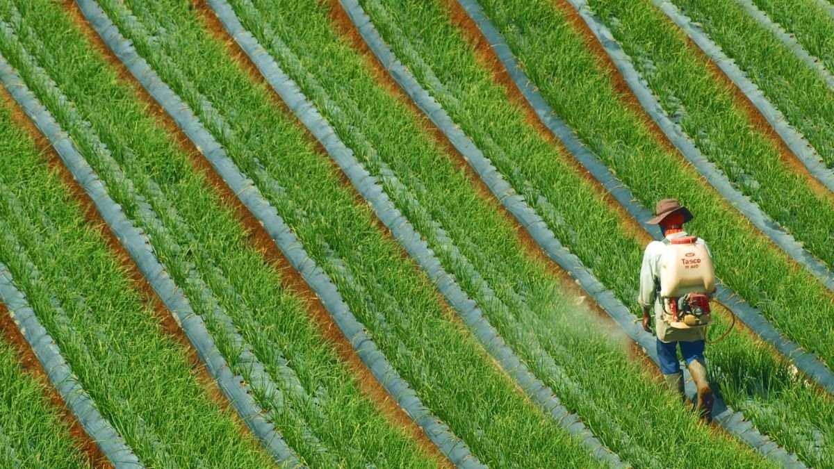
For a farmer, fertilizer is not just another item in the supply chain. It can determine how much a crop grows, how much it costs to cultivate and, ultimately, how much a family earns from a harvest. For the government, however, it is also a massive logistical and financial exercise. Millions of tonnes have to reach farmers on time, while subsidies worth thousands of crores have to be tracked.
India is now trying to bring these two sides closer through data. The Integrated Fertilizer Management System (iFMS), the government’s digital platform for managing its production, imports, stocks, sales and subsidies, is being expanded to connect fertilizer purchases with information about farmers, land and crops. It already covers more than 14 crore Aadhaar-linked buyers, over 2.5 lakh retailers and around 7 crore fertilizer transactions every year.
If the government knows what farmers are buying, where they farm and what they are growing, it could get a clearer picture of how much fertilizer is actually needed. But, can better data change the way it is used, or will it simply make the existing system easier to monitor?
Tracking and Understanding its Use
Until now, much of iFMS has focused on following fertilizer through the system—from production and imports to retailers and sales. That is changing. New analytical tools can examine it’s purchases by crop, district, landholding and the type. The government says this can help identify unusual consumption patterns and emerging supply problems. The new Framework for Fertilizer Sale goes a step further. A farmer can book fertilizer using an AgriStack-linked identity after their land and ownership details are verified. A QR-based booking is then generated and matched with the eventual purchase at the retailer. The system can compare what the farmer said they needed with what they actually bought.
In theory, this gives policymakers a much clearer picture. Instead of simply knowing that a certain amount of fertilizer was sold in a district, they could begin asking: Which crops are using it? How much is being applied per hectare? And does the amount purchased make sense for the recorded farm and crop?
That could help with planning supplies and identifying unusual patterns. The government is also using vehicle-location tracking to follow its consignments while they are being transported. This is intended to make it easier to identify delays and unusual movement. For a country managing a huge fertilizer subsidy bill, that visibility matters. But fertilizer shortages and supply-chain leakages are only part of India’s fertilizer problem.
The Problem is Also What Farmers are Encouraged to Use
India has struggled for years with an imbalance in fertilizer use. One reason is price. Urea is sold at a controlled price, while several other fertilizers are covered under the Nutrient Based Subsidy system. This has contributed to a strong preference for nitrogenous fertilizer, particularly urea. PRS has highlighted the resulting imbalance as a concern for agricultural sustainability. But farmers do not make fertilizer decisions based on national nutrient ratios alone.

Their choices are influenced by crop, soil, price, availability, weather and advice from agricultural extension systems. This is why simply collecting more purchase data will not necessarily change fertilizer use. The real value of the system would come if that information could help connect what farmers are buying with what their crops and soils actually need.
ICAR has continued to emphasise balanced nutrient management and soil-test-based fertilizer recommendations as important for maintaining soil health and improving fertilizer efficiency.
What Happens When the Data is Wrong?
There is another issue that could determine whether the system works at the farm level: the quality of the data itself. The government acknowledges that its earlier efforts to connect fertilizer transactions with farmer, land and crop records exposed problems with the availability, completeness and quality of that information.
That matters because a digital record is only useful if it accurately describes the farm. A farmer may change crops. Land records may not reflect current cultivation. Agricultural land can be divided, leased or cultivated under arrangements that are not always captured neatly in administrative databases. If the information is outdated, the system may arrive at an “assessed requirement” that does not match what the farmer actually needs.
And that term—assessed requirement—is becoming important under the new framework. The system is designed to compare fertilizer requirements indicated during booking with actual purchases.
It Cannot Replace Agricultural Knowledge.
India already has several pieces of the puzzle. Soil testing can provide information about nutrient requirements. Crop data can show what is being cultivated. The purchase data can show what farmers are actually using. Logistics data can show where supplies are moving. Bringing these datasets together could help governments identify where fertilizer use is persistently high, where certain nutrients are underused and where farmers may need better agricultural advice.
But the system should not assume that more data automatically means better decisions. Indian agriculture varies enormously across regions. A fertilizer practice that makes sense for one crop or soil may not make sense for another. The government’s own experience with land and crop data shows why this matters. The challenge, therefore, is not simply building a larger database. It is making sure that the database reflects what is happening on the ground.
The Bigger Shift
The latest changes to iFMS point to a larger transformation in agricultural governance. The system is increasingly connecting production, imports, logistics, stocks, farmer and land information, fertilizer bookings, retail sales and subsidy payments. That could give policymakers something they have often lacked: a more detailed picture of how it moves from the supply chain to the farm.
But the success of this system is judged only by whether it can help India use fertilizer more efficiently, protect soil health and ensure that farmers receive what they actually need. For that to happen, the data must be accurate, farmers must be correctly represented in the system and digital assessments must account for the realities of farming. The next challenge is turning that information into better decisions—for farmers, for the soil and for the food system.


India’s New Satellite Will Be Tested During Disasters

The Himalayas Are Under Pressure From Above, Below and Within

Lise Meitner: a Physicist Who Never Lost Her Humanity

560 Million Children, One Overheating Planet

If AI Can Explain Everything, What Is Left for a Teacher to Teach?

Astronomers Discover a ‘Black Hole Star’, a New Kind of Object in the Early Universe

From Bell Labs to the Classroom: Finding Purpose After Retirement

From Soil to Profit: How Organic Turmeric Changed the Fortunes of a Tribal Farming Family

Farmers Borrowed to Build ‘Diggis’. Two Years Later, They Are Still Waiting for the Subsidy

Our Algorithm Knows What We Want Before We Do. That is the Problem.

-

 Math1 month ago
The 2026 Fields Medals: Four Proofs, Four Decades-Old Problems Solved
-
Climate1 month ago
After Kerala’s Deadliest Landslide, the Hardest Thing to Rebuild Was Childhood
-
Society2 months ago
West Asia Crisis: Can Kerala’s Returning Gulf Migrants Find a Future in the Green Economy?
-
Space & Physics3 months ago
India Semiconductor Mission: ‘It’s Not About Fabs. It’s About Building An Entire Ecosystem’
-
Climate3 months ago
The Climate World Cup? How Climate Change Could Affect Player Performance at the 2026 World Cup
-
Society2 months ago
What Is Civilisational Diplomacy? Understanding India’s Newest Foreign Policy Tool
-
Society3 months ago
From Bell Labs to the Classroom: A Second Career in Teaching
-
Space & Physics3 months ago
Engineers Develop Dual-Mode Propulsion System for Next-Generation Small Satellites