
Technology
Neuropixels Probes Allow Scientists to Record Hundreds of Brain Cells at Once, Opening New Possibilities for Neuroscience
Neuropixels technology is transforming neuroscience by helping researchers monitor hundreds of individual neurons simultaneously and investigate how the brain processes information.


Understanding how the human brain processes information requires scientists to observe the activity of individual neurons and the connections between them. However, recording electrical signals from large numbers of these cells simultaneously has remained a technical challenge.
A technology called Neuropixels is helping researchers overcome this limitation. Developed initially for neuroscience experiments in animals, these extremely thin silicon probes can record electrical activity from hundreds of neurons simultaneously. Their use is now expanding into human research, where they could help scientists investigate brain functions at a level of detail that was previously difficult to achieve.
How Do Neuropixels Probes Work?
Neurons communicate through electrical signals. When a neuron becomes active, it produces a brief electrical impulse known as an action potential. Recording these impulses allows researchers to study when individual neurons fire and how their activity relates to other cells.
Traditional electrode systems had limitations in the number of neurons they could monitor simultaneously. Researchers commonly used electrodes that recorded from a few dozen channels, making it difficult to study activity across several brain regions at once.
Neuropixels uses a thin silicon probe containing hundreds of closely spaced recording sites. These sites detect electrical signals from nearby neurons, while integrated electronics amplify and convert the signals into digital data that researchers can analyse. The first Neuropixels 1.0 probe, developed through a collaboration between researchers at the Howard Hughes Medical Institute’s Janelia Research Campus and Belgium’s Interuniversity Microelectronics Centre (Imec), was reported in 2017.
It contained 960 recording sites along a hair-thin silicon shaft, with 384 channels capable of reading signals simultaneously. In early experiments, researchers inserted two probes into a mouse brain and recorded activity from approximately 700 neurons across five brain regions. Neuropixels 2.0 followed in 2021. Its four-shank version contains 5,120 recording sites, of which 1,536 can be read out simultaneously. The smaller and lighter design also supports longer-term recordings in small animals.
What are the Possibilities of the Technology?
Neuropixels has helped researchers study how different regions of the brain coordinate during sensory processing, movement and decision-making. Earlier experiments often examined relatively small groups of neurons. Recording larger populations has revealed that some brain functions are distributed across several regions rather than confined to a single location.
The technology has also helped scientists investigate neural manifolds, mathematical patterns formed by the collective activity of populations of neurons. Studying these patterns can provide insights into how the brain represents information and organises its activity. One major effort involved the International Brain Laboratory, a collaboration of 12 research laboratories in the United States and Europe.
In a 2025 study, researchers recorded activity from more than 620,000 neurons across 279 brain regions in 139 mice. The resulting dataset provided a large-scale map of neural activity associated with functions including vision, movement and decision-making. Neuropixels is now being used in more than 1,700 laboratories worldwide and has been applied to over two dozen species, including zebra finches, bearded dragons and octopuses.
To Human Brain Research
One of the most significant developments is the technology’s entry into human neuroscience. Researchers at the National Hospital for Neurology and Neurosurgery in London have been working with neurosurgeons to use Neuropixels probes during brain operations.

In one procedure described by Nature, a patient undergoing surgery for normal pressure hydrocephalus, a condition involving excess cerebrospinal fluid inside the skull, agreed to participate in a research experiment.
During the operation, researchers briefly inserted a probe into her brain to record neuronal activity. They played sequences of familiar and unfamiliar word combinations to examine how the brain responded to changes in auditory stimuli.
The recordings allowed researchers to observe electrical responses from individual neurons as the patient received the sounds. Human brain research has traditionally relied on techniques such as electrocorticography, which measures electrical activity through electrodes placed on the brain’s surface. Other devices can record activity at the single-neuron level, but generally monitor fewer cells.
Neuropixels offers a more detailed approach by allowing researchers to examine the activity of large numbers of individual neurons simultaneously. The technique is particularly valuable because some existing imaging methods, including calcium imaging, cannot capture the rapid electrical activity of neurons with the same temporal resolution. Calcium imaging also relies on genetically encoded sensors in many experimental settings, limiting its application in humans.
Understanding Brain Disorders
The ability to monitor individual neurons across larger brain networks could help researchers investigate how changes in neural activity contribute to neurological and psychiatric conditions. Diseases such as Alzheimer’s involve changes in brain cells and the circuits connecting them. Understanding how these changes affect communication between neurons could provide important information about disease progression and the development of potential treatments.
Neuropixels is already being used in research examining neural circuit activity in animal models of neurodegenerative conditions. Its expansion into human research could eventually help scientists compare findings from animal experiments with neuronal activity recorded directly from patients.
However, the technology remains a research tool. Its use during surgery is still developing, and further work is needed to establish safe and reliable procedures for different research applications. The recordings themselves do not diagnose brain disorders or provide an immediate treatment.
For now, the major contribution of Neuropixels is the scale and precision of the information it can collect. By allowing scientists to follow the electrical activity of large populations of individual neurons, it is helping them investigate how the brain processes information through interconnected networks of cells.






Technology
New Semiconductor Could Help Make Solar Cells More Efficient, Oxford Study Finds
Researchers from the University of Oxford and Wuhan University have identified bismuth sulfide as a semiconductor material that could overcome a longstanding trade-off between light absorption and electrical charge retention in solar energy conversion.

Researchers from the University of Oxford and Wuhan University have identified a semiconductor material that could help overcome a longstanding limitation in solar energy conversion. The study, published in Nature on October 28, 2026, demonstrates how bismuth sulfide can absorb light strongly while slowing the loss of electrical charges generated during the process.
The discovery could offer a new direction for developing solar cells that convert sunlight into electricity more efficiently. It challenges the conventional understanding that materials with stronger light absorption necessarily lose their electrical charges more rapidly.
Solar cells use semiconductor materials to absorb sunlight and generate electrical charges. When sunlight strikes a semiconductor, it releases negatively charged electrons, leaving behind positively charged gaps known as holes. These charges must reach the electrodes to generate electricity. However, electrons and holes can recombine before being collected, releasing their energy and reducing the amount available for electricity generation.
This process, known as electron-hole recombination, is a major source of energy loss in solar cells. Materials that absorb sunlight efficiently often experience faster recombination, while those that retain electrical charges for longer periods generally have weaker light absorption. This trade-off has restricted the development of materials that combine both properties.
How bismuth sulfide slows electrical charge loss
The researchers found that bismuth sulfide (Bi₂S₃) combines characteristics of two conventional semiconductor types: direct and indirect semiconductors. Direct semiconductors absorb light strongly but generally allow electrons and holes to recombine quickly. Indirect semiconductors have slower recombination rates but weaker light absorption.
Bismuth sulfide exhibits a combination of these properties. The researchers describe it as a pseudo-direct semiconductor, in which closely spaced electronic energy levels allow the material to absorb light strongly while providing a lower-energy pathway that slows electrical charge recombination.
To investigate this mechanism, the team studied thin films of bismuth sulfide using ultrafast terahertz spectroscopy. By exciting the material with extremely short laser pulses, researchers measured the behaviour of the resulting electrical charges across different temperatures.
The findings, supported by electronic-structure calculations, showed that the material’s unusual electronic arrangement could reduce the rate of electron-hole recombination by approximately 75% at room temperature compared with conventional materials having similar light absorption.
Slower recombination could give electrical charges more time to reach the electrodes, potentially reducing energy losses during electricity generation. The researchers also suggest that the mechanism could be relevant to solar fuel technologies, where sunlight is used to drive chemical reactions.
Building on advances in solar-cell materials
The findings add to ongoing research aimed at improving solar-cell performance by controlling charge-carrier recombination. A study published in Nature Photonics in 2025 demonstrated how surface engineering could reduce recombination losses and improve the stability of perovskite solar cells.
By introducing sodium heptafluorobutyrate to modify the perovskite surface, researchers achieved a certified power-conversion efficiency of 26.96%. The devices retained their initial efficiency after 1,200 hours of continuous illumination and maintained 92% of their initial efficiency after 1,800 hours of ageing at 85°C.
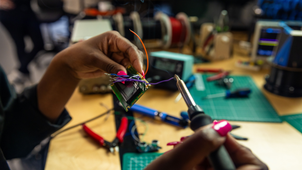
Representative image.Image credit:Pexels
While the two studies use different approaches, they highlight the importance of controlling electrical charge losses in developing more efficient and stable solar technologies.
The Oxford researchers suggest that other materials, including tungsten diselenide and indium selenide, could be investigated for similar electronic properties. They also propose that techniques such as stretching layered crystals could help modify the energy levels of certain semiconductors.
However, the discovery does not mean that more efficient commercial solar panels are immediately within reach. The Oxford study establishes the physical mechanism in bismuth sulfide thin films rather than demonstrating a complete solar cell with improved power-conversion efficiency. Further research will be needed to assess its performance, stability and manufacturing potential.
By showing how strong light absorption can coexist with slower electrical charge recombination, the research offers a new direction for identifying semiconductor materials for future solar energy technologies.
The Sciences
MIT Researchers Develop Origami-Based Method for Lightweight, Load-Bearing Structures
MIT researchers have developed an origami-inspired construction technique that could enable lightweight, rigid structures using less material and simpler assembly methods.

Researchers at the Massachusetts Institute of Technology (MIT) have developed an origami-inspired construction method that could enable the fabrication of lightweight, rigid structures using less material and simpler assembly techniques. The approach could eventually be used for emergency shelters, architectural components and lightweight aerospace parts.
The modular system uses components cut from flat sheets of material, folded into shape and connected to form three-dimensional structural shells. According to MIT, simulations indicate that the structures can be approximately 3.5 times stiffer than those produced using some other structural origami techniques, while requiring only about two-thirds as much material.The research was announced by MIT on October 27 and published in the International Journal of Solids and Structures.
Building structures through folding
The researchers drew inspiration from geometric patterns developed by artist and scientist Ron Resch in the 1960s. Unlike methods that fold a single sheet into a complete structure, the new approach uses individually fabricated components that are folded and connected to create a larger framework.
Alfonso Parra Rubio, a graduate student at MIT’s Center for Bits and Atoms and lead author of the study, developed a method for combining two tripod-shaped units into a rigid building block. These blocks can be interconnected to form a network of beams that creates a lightweight structural shell.
To simplify the design process, the team developed computational software that automatically generates components according to the intended structure. The software checks whether individual units can be folded before combining them into the final design.
The resulting files can be sent to computer-controlled cutting equipment to manufacture components from flat sheets of material, including aluminium. Workers can then fold and assemble the units using basic hand tools, without requiring large-scale welding equipment.
Demonstration at architectural scale
To demonstrate the method’s scalability, the researchers constructed a 23-foot folded-aluminium sculpture that was installed in the atrium of the Boston Public Library. According to MIT, a team without professional construction experience assembled the structure in a matter of days.
The researchers say the modular design simplifies assembly because the components are engineered to fit into their intended positions as the structure takes shape.

Representational image.Image credit:Pexels
However, the reported stiffness improvements are based on simulations comparing the method with other origami-based systems. Further testing will be necessary to establish its performance across different materials, loading conditions and real-world construction environments.
Potential applications
One potential application is disaster-relief housing. Flat-packed components could be transported efficiently to areas affected by earthquakes or floods and assembled on site, potentially reducing transportation and construction requirements.
The approach could also be explored for lightweight aerospace components, modular robots, sound-dampening panels and building facades. Its ability to create rigid structural shells without interior support columns could offer additional flexibility in architectural design.
The researchers plan to test the technique in larger architectural structures and investigate more complex component geometries that could improve strength and stiffness. They also intend to develop a more accessible interface for designing structures using the system.
While the method has yet to demonstrate widespread use in buildings, the research illustrates how geometric design and digital manufacturing could offer alternatives for constructing complex structures.
Its practical adoption will depend on factors including durability, manufacturing costs, structural safety and performance under real-world conditions. Nevertheless, the approach presents a potential option for applications where reducing material use and simplifying assembly are priorities.
Technology
India’s Electronics Boom Masks a Deeper Dependence on Semiconductor Imports
India’s semiconductor industry is expanding, but dependence on imported chips remains a major challenge. New investments and manufacturing initiatives aim to strengthen domestic production and build a more resilient electronics supply chain.

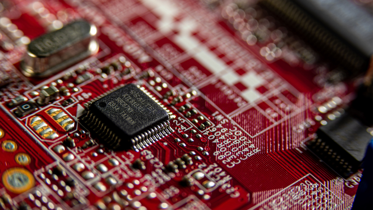
India’s electronics manufacturing industry is expanding rapidly, but its dependence on imported semiconductors remains a significant challenge. A new industry report highlights the gap between the country’s growing electronics production and its efforts to establish a self-reliant semiconductor ecosystem.
India’s annual semiconductor import bill has reached ₹2.8785 lakh crore, according to the State of India’s Semiconductor Industry 2026 report released by the Data Security Council of India (DSCI) on October 23. The report estimates that India continues to depend on imports for 90–95 per cent of its semiconductor requirements.
The findings underline a central challenge in India’s technology ambitions: expanding the production of electronic devices while reducing dependence on foreign suppliers for the chips and components that power them.
Electronics production rises, but dependence persists
India’s electronics manufacturing industry has grown considerably over the past decade. According to government figures, electronics production increased from approximately ₹1.9 lakh crore in 2014–15 to ₹13.11 lakh crore in 2025–26. Electronics exports rose from around ₹38,000 crore to ₹4.24 lakh crore over the same period.
However, growth in electronics manufacturing does not necessarily mean that the components used in these products are manufactured domestically.
Semiconductors are essential to smartphones, computers, automobiles, telecommunications equipment and data centres. Their production involves complex processes requiring specialised facilities, advanced equipment, materials and highly skilled workers.
India has developed a substantial electronics assembly and manufacturing base, but building a semiconductor ecosystem requires investment across several stages, from chip design and wafer fabrication to assembly, testing and packaging.
The distinction matters because a country can manufacture and export electronic devices while continuing to import many of the high-value components used in them. Reducing semiconductor imports therefore requires strengthening domestic production capabilities rather than simply increasing the number of devices assembled within the country.
Five manufacturing units enter production
India launched the Semicon India Programme in 2021 with an initial outlay of ₹76,000 crore to establish a domestic semiconductor and display manufacturing ecosystem.
According to government figures and the DSCI report, 12 semiconductor manufacturing projects have been approved, involving investments exceeding ₹1.64 lakh crore. Five units have commenced commercial production.
The approved projects include silicon and silicon carbide fabrication facilities, a gallium nitride micro-LED display facility, and nine units focused on assembly, testing and packaging.
These facilities represent an important step towards establishing domestic semiconductor manufacturing capacity. However, the commencement of production does not, by itself, establish how much domestic demand the facilities can meet or how quickly they can reduce import dependence.
The government approved Semicon 2.0 in July 2026 with an outlay of ₹1,27,500 crore. The programme aims to strengthen research and development, chip design, manufacturing equipment, materials, workforce development and advanced packaging.
The broader objective is to develop an ecosystem in which domestic manufacturers can access more of the infrastructure and specialised services required to produce semiconductors.
Strengthening the supply chain
Semiconductor manufacturing depends on more than fabrication plants. It requires specialised materials, sophisticated machinery, reliable infrastructure, research capabilities and trained personnel.
A May 2026 roadmap by NITI Aayog identified India’s dependence on imported semiconductors and components as a vulnerability, particularly given the concentration of global manufacturing capacity in a limited number of countries.
Supply disruptions can affect industries ranging from automobiles and consumer electronics to telecommunications and defence. A shortage of critical chips can interrupt production even when manufacturers have sufficient capacity to assemble the final product.
India’s policy response has consequently extended beyond semiconductor fabrication. The Electronics Component Manufacturing Scheme seeks to develop domestic suppliers and strengthen the production of components used across the electronics industry.
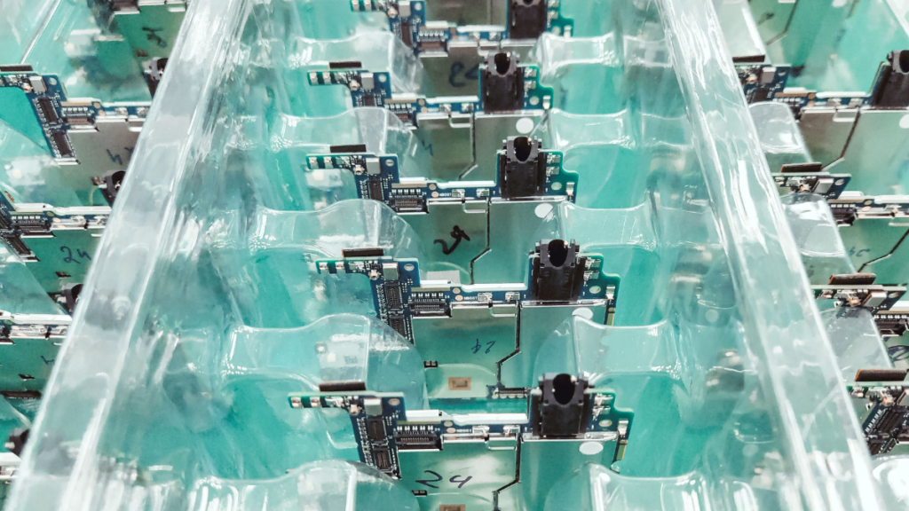
Detailed view of organized electronic circuit boards in a production setting.Image credit:Pexels
Government figures published in September indicated that 106 projects had been approved under the scheme by August, with 38 approved plants already producing components.
Developing these supporting industries could help domestic manufacturers access more components locally. Nevertheless, the extent to which this reduces semiconductor dependence will depend on the types of components produced, their quality, cost and ability to meet industrial demand.
The workforce challenge
India’s established strength in semiconductor design offers another opportunity. The country has a large pool of engineers working in chip design and related technology services. Translating this advantage into manufacturing capacity, however, requires additional skills and infrastructure.
Operating semiconductor fabrication facilities involves specialised knowledge of materials, manufacturing processes, equipment maintenance and quality control. Assembly, testing and packaging also require trained technicians and engineers.
The DSCI report identifies workforce development as a priority, including the need to train approximately one lakh factory-floor technicians.
Such training will be essential if new facilities are to operate efficiently and expand production. Collaboration between industry, technical institutions and research organisations could help address the skills gap, although the availability of trained personnel alone cannot guarantee commercially competitive manufacturing.
Beyond factory announcements
India’s semiconductor ambitions reflect a wider effort to strengthen technological security and reduce exposure to international supply disruptions. Yet progress cannot be measured solely by the number of approved projects or the investments announced.
The more significant indicators will be sustained commercial production, manufacturing yields, domestic value addition, the development of local suppliers and the ability to meet demand at competitive prices.
India’s expanding electronics exports demonstrate the strength of its manufacturing growth. Its semiconductor import bill, meanwhile, illustrates the gap between assembling electronic products and producing the critical components within them.
Bridging that gap will require sustained investment in research, infrastructure, skilled labour and the supporting industries that make semiconductor production possible. Whether India’s new manufacturing projects can translate policy ambitions into a resilient domestic supply chain will determine how far the country can move towards semiconductor self-reliance.


Indian universities lead Asia in research output per faculty, but the country’s top six all slip in QS ranking

Greener Forests, Weaker Carbon Sinks? Study Finds Declining Productivity in Northeast India

Climate Change Contributed to 10,600 Excess Preterm Births in Asia During April 2024 Heatwave

Neuropixels Probes Allow Scientists to Record Hundreds of Brain Cells at Once, Opening New Possibilities for Neuroscience

Overshooting 1.5°C Could Trigger Irreversible Damage to Earth’s Ice Systems, Warns UN-Backed Report

Knowing When to Think for Ourselves: AI, Intuition and the Education of Discernment

After a Scorching Summer, Delhi’s Children Are Slow to Return Outdoors

Two Chemists Win Nobel Prize for Solving a Century-Old Puzzle: Why Life Picks One Hand Over the Other

Climate Change, Overfishing and the Uncertain Future of Bangladesh’s Hilsa Fishermen

Europe Braces for Extremes as Commission Unveils Climate Resilience Framework

-

 Math3 months ago
The 2026 Fields Medals: Four Proofs, Four Decades-Old Problems Solved
-
EP Deep Dive: Data & Solutions3 months ago
After Kerala’s Deadliest Landslide, the Hardest Thing to Rebuild Was Childhood
-
EP Deep Dive: Data & Solutions4 months ago
West Asia Crisis: Can Kerala’s Returning Gulf Migrants Find a Future in the Green Economy?
-
Space & Physics5 months ago
India Semiconductor Mission: ‘It’s Not About Fabs. It’s About Building An Entire Ecosystem’
-
Interviews1 month ago
From Scams to Screens: How the National Stock Exchange Rewrote India’s Equity Story
-
Climate5 months ago
The Climate World Cup? How Climate Change Could Affect Player Performance at the 2026 World Cup
-
Society4 months ago
What Is Civilisational Diplomacy? Understanding India’s Newest Foreign Policy Tool
-
Society5 months ago
From Bell Labs to the Classroom: A Second Career in Teaching