
Space & Physics
What brought carbon to Earth
This marks the first time a complex form of carbon essential for life on Earth has been observed outside the solar system. To learn more about the significance of this discovery, EdPublica interviewed the researchers behind the study– Gabi Wenzel, Ilsa Cooke, and Brett McGuire, who shared their insights on the implications of pyrene’s presence in space and its potential impact on our understanding of star and planet formation

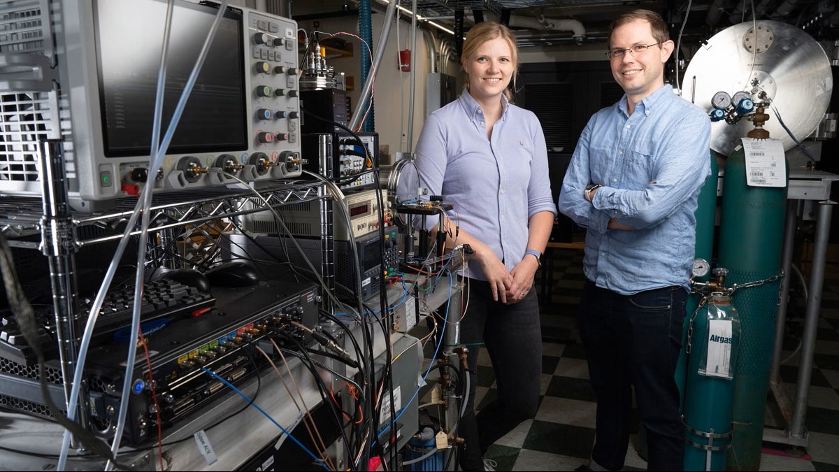
A team led by researchers at MIT has detected pyrene, a complex carbon-containing molecule, in a distant interstellar cloud. This finding opens new avenues for understanding the chemical origins of our solar system. Pyrene, a type of polycyclic aromatic hydrocarbon (PAH), was found in a molecular cloud similar to the one from which our solar system formed.
This marks the first time a complex form of carbon essential for life on Earth has been observed outside the solar system. Its discovery sheds light on how the compounds necessary for life could originate in space. The team detected pyrene in
a star-forming region known as the Taurus Molecular Cloud, located 430 light-years away, making it one of the closest such clouds to Earth.
This discovery also aligns with recent findings from the asteroid Ryugu, suggesting that pyrene may have played a key role in the carbon composition of the early solar system. To learn more about the significance of this discovery, EdPublica interviewed the researchers behind the study– Gabi Wenzel, Ilsa Cooke, and Brett McGuire, who shared their insights on the implications of pyrene’s presence in space and its potential impact on our understanding of star and planet formation. Brett McGuire is an assistant professor of chemistry at MIT, Ilsa Cooke is an assistant professor of chemistry at the University of British Columbia, and Gabi Wenzel is a postdoctoral researcher in McGuire’s group at MIT.
Below, the team responds to questions from EdPublica Editor Dipin Damodharan about this unexpected and exciting discovery.
‘Pyrene could be a major source of carbon in our solar system’
Q: How does the discovery of pyrene in TMC-1 enhance our understanding of the chemical inventory that contributed to the formation of our solar system?
Gabi Wenzel:
Stars much like our own sun are born from dense molecular clouds. The discovery of pyrene in a molecular cloud called TMC-1, one that might be very similar to our sun’s natal cloud and which will go on to form a star of its own, significantly enhances our understanding of the chemical inventory that contributed to the formation of our own solar system. As a polycyclic aromatic hydrocarbon (PAH), pyrene is one of the most complex organic molecules found in early molecular clouds, suggesting that the building blocks of organic matter were available in the environments where stars and their orbiting (exo)planets form.

This discovery sheds light on the chemical processes occurring in interstellar space, including gas-phase and surface reactions on dust grains, which are crucial for the evolution of organic chemistry. This further supports the notion that the primordial materials of our solar system contained a diverse range of organic compounds, providing insights into the potential for prebiotic chemistry on a young Earth and planetesimals.
Q: What specific challenges did you face in detecting pyrene, given that it is invisible to traditional radio astronomy methods, and how did the use of cyanopyrene help overcome these challenges?
Gabi Wenzel:
Pyrene, a fully symmetric PAH, does not possess a permanent electric dipole moment and hence is invisible in radio astronomical observations or rotational spectrometers in the laboratory. The CN radical is highly abundant in the cold and dark molecular cloud TMC-1, an environment that is about 10 K cold and in which you’d assume little chemistry to happen. However, earlier experimental works have shown that the CN addition (followed by hydrogen abstraction) to ringed hydrocarbon species such as benzene and toluene at low temperatures is a barrierless process.
Adding a CN (nitrile) group to a hydrocarbon will drastically increase its permanent electric dipole moment and so allow rotational transitions. Indeed, several CN-functionalized species have been detected in TMC-1 and other sources, among which the CN-substituted benzene (cyanobenzene or benzonitrile) and other smaller PAHs, with cyanopyrene being the largest molecule found via radio astronomy to date, allowing us to infer the presence of pyrene itself.
Q: Can you elaborate on what it means for our understanding of carbon sources in the solar system that pyrene is found in both TMC-1 and asteroid Ryugu?
Ilsa Cooke:
TMC-1 is a famous example of a cold molecular cloud, one of the earliest stages of star and planet formation, while asteroids like Ryugu represent snapshots of later stages in the formation of solar systems. Asteroids are formed from material in the solar nebula that was inherited from the molecular cloud stage. Our radio observations of TMC-1 let us observe pyrene early on and possibly under conditions where it is first forming. Isotope signatures of the pyrene in Ryugu suggest it was formed in a cold interstellar cloud. From these two unique sets of measurements, we can start to unravel the inheritance of pyrene, and PAHs more generally, from their birth in interstellar space and their journey to new planets. If PAHs can survive all the way from the molecular cloud stage, they may provide planets with an important source of organic carbon.

Q: What are the different formation routes of PAHs that your research suggests, and how do these differ from previous hypotheses about PAH formation in space?
Ilsa Cooke:
Our results, combined with those of Zeichner et al., who measured pyrene in Ryugu, suggest that pyrene may form at low temperatures by “bottom-up” routes in molecular clouds. Previously, PAHs were most commonly associated with formation in high-temperature (ca. 1000 K) environments in the envelopes of dying stars. These stars are thought to eject their PAHs, along with other carbon-rich molecules, into the diffuse interstellar medium.
However, the diffuse medium is a tenuous, harsh environment permeated by ultraviolet photons, and most astrochemists think that small PAHs would not survive their journey through the diffuse medium into dense molecular clouds. So we are still left with a puzzle: does that pyrene that we observe in TMC-1 form there, or was it formed somewhere else but it was able to survive its journey more efficiently than previously thought? If the pyrene is indeed formed within TMC-1, we do not yet know the chemical mechanism. Many possibilities exist, so close collaborations between laboratory astrochemists and observers will be critical to answer this question.

Q: What are your plans for investigating larger PAH molecules in TMC-1, and what specific hypotheses are you looking to test with these investigations?
Brett McGuire:
We have a number of other targets lined up – again focusing on PAH structures that should show this special stability demonstrated by pyrene. They present the same experimental challenges, including needing to devise appropriate synthetic routes in the laboratory before collecting their spectra. The major question is just how complex the PAH inventory actually gets at this earliest stage of star formation.

Prior to our work in TMC-1, nearly everything we knew about PAHs came from infrared observations of bulk properties in much warmer and more energetic regions, where PAHs are thought to be much larger. Does the population in TMC-1 look the same as in these regions? Is it at an earlier stage of chemical evolution? And how does this distribution compare to what we see in our own Solar System?
Q: How do your findings about pyrene and PAHs in interstellar clouds influence our broader understanding of organic chemistry in the universe, particularly in relation to the origins of life?
Brett McGuire:
Life as we know it depends on carbon – it is the backbone upon which all our molecular structures are constructed. Yet, the Earth overall is somewhat depleted in carbon relative to what we’d naively expect, and we still don’t fully understand where the carbon we do have came from originally. PAHs in general seem to be a massive reservoir of reactive carbon, and what we are now seeing is that that reservoir is already present at the earliest stages of star-formation. Combined with the evidence from Ryugu, we’re now also seeing indications that the inventory of PAHs, and thus this reservoir of carbon, may actually survive from this dark molecular cloud phase through the formation of a star to be eventually incorporated into the planetary system itself.












Space & Physics
How Scientists Traced the Flow of Matter Around a Dead Star Using X-rays
By studying changes in X-ray signals from Centaurus X-3, researchers at Bengaluru’s Raman Research Institute have found evidence of an unusual way in which matter reaches a neutron star. The discovery could change how scientists explain the radiation coming from this distant system.

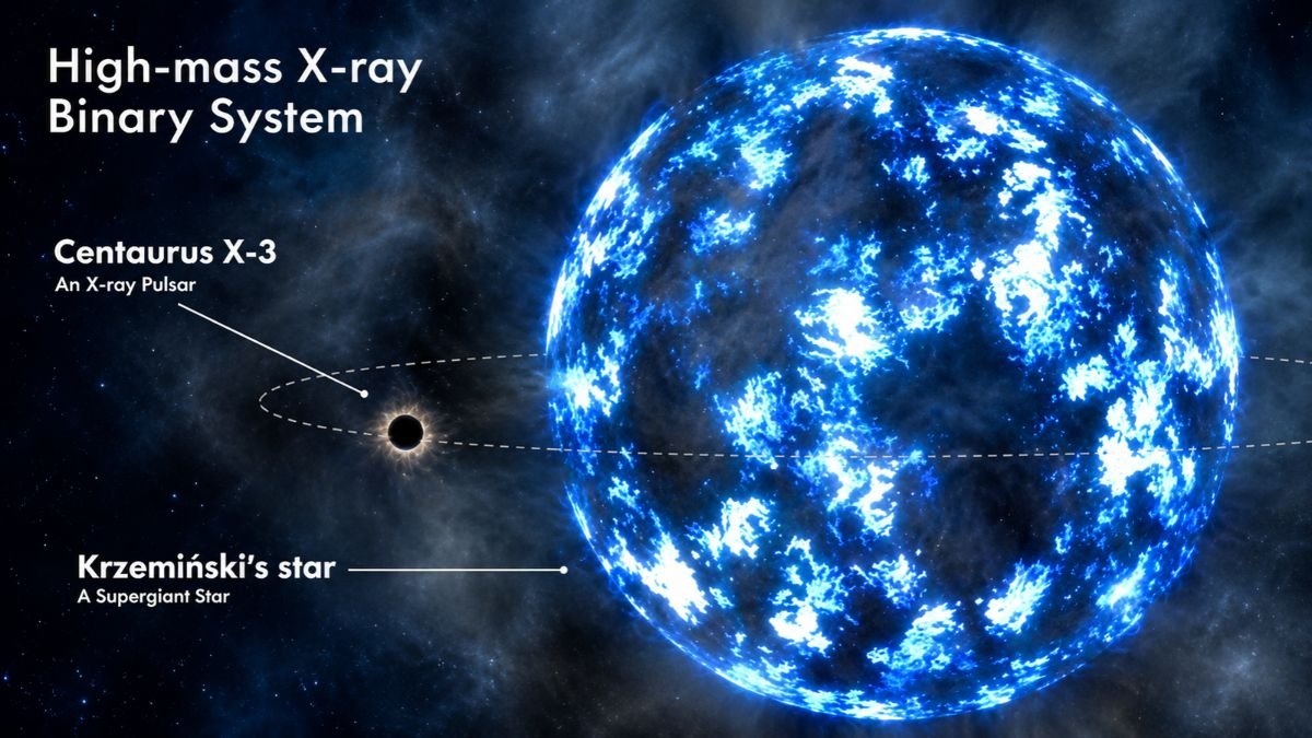
When a massive star dies, its core can collapse into an extremely dense object called a neutron star. Despite being only about the size of a city, it can have a mass comparable to that of the Sun. Its powerful gravity can pull matter away from a nearby companion star, releasing energy in the form of X-rays as the material falls towards it.
Scientists at Bengaluru’s Raman Research Institute (RRI) have studied these X-ray signals from Centaurus X-3, a star system about 24,000 light-years from Earth. By examining changes in the signals, the researchers identified a stream of matter flowing towards the neutron star and found evidence of a rotating disk of material around it. This is an unusual finding because such disks are not commonly expected in this type of star system. The discovery could help scientists better understand how matter moves around neutron stars and how these distant objects produce X-rays.
Star That Pulls in Matter
Centaurus X-3 is in the constellation Centaurus. It belongs to a class of systems known as high-mass X-ray binaries. These systems contain a neutron star and a massive companion star held together by gravity.
A neutron star forms when the core of a massive star collapses at the end of its life. It packs roughly the Sun’s mass into a sphere only about the size of a city. Its gravity is so strong that it can pull in material from a nearby companion star. As this material falls towards the neutron star, it releases enormous amounts of energy, including X-rays. Scientists study this radiation to understand how the material behaves and how the system works.
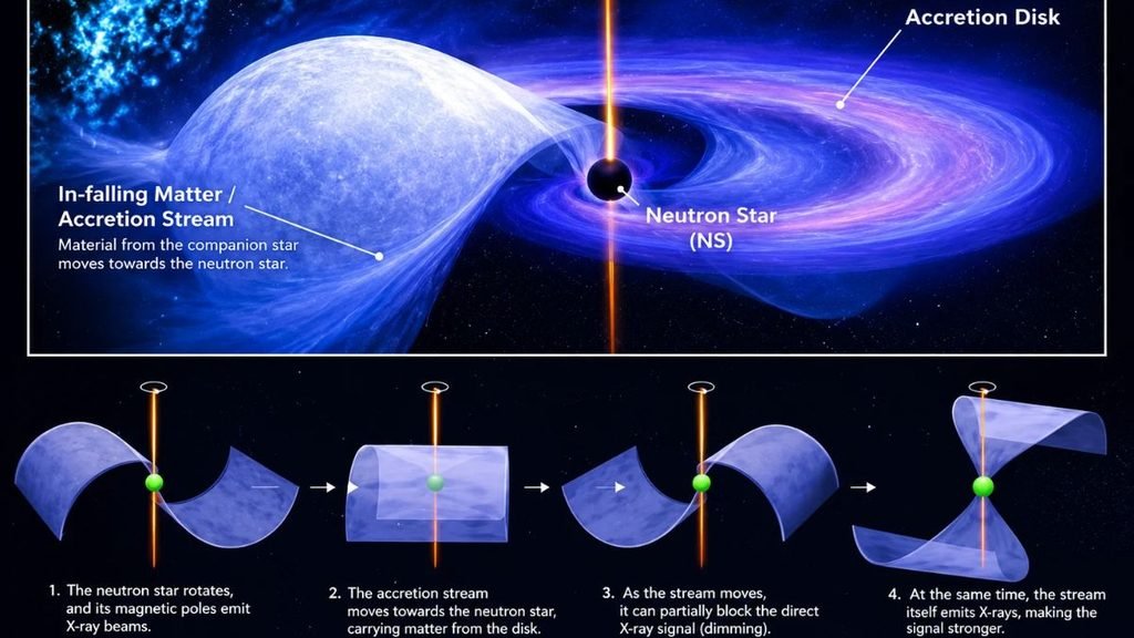
Centaurus X-3 is also a pulsar. Its neutron star rotates and sends out radiation from regions near its magnetic poles. As the star spins, these beams sweep across space. When a beam passes an observing satellite, the satellite detects a pulse of radiation, much as a lighthouse produces a repeating flash as it turns. These regular pulses provide scientists with a way to study the neutron star and its surroundings.
What the Changing Signals Revealed
The radiation from Centaurus X-3 does not come only from the neutron star itself. Some of it interacts with nearby material, including the surface of the companion star, gas flowing away from it and matter surrounding the neutron star. This material absorbs radiation and emits it again. Scientists call this secondary radiation.
Changes in this radiation can help researchers work out what is happening around the neutron star. However, Centaurus X-3 is so far away that telescopes cannot clearly distinguish its surrounding structures. It appears as a single point of light. Scientists must therefore piece together the system’s structure from the signals they receive.
Earlier observations had shown that the intensity of certain secondary X-ray emission lines changed as the neutron star rotated. An emission line is a feature in a spectrum that can reveal information about the material producing or interacting with the radiation. A research team led by Kinjal Roy of RRI examined four such emission lines in detail. The researchers found that the structure producing these changes must be rotating along with the neutron star.
The pattern helped them identify the likely source which is a stream of matter moving towards the neutron star.
Following the stream of matter
This stream is part of a process called accretion, in which a compact object draws in material from its surroundings. In Centaurus X-3, the stream carries matter from an accretion disk towards the neutron star. The disk is a rotating structure of gas and other material that moves around the star before being drawn inwards. The neutron star’s magnetic field then guides the incoming matter towards its magnetic poles.
The stream also changes what an observing satellite sees. As it moves around the neutron star, it can come between the satellite and the star, partially blocking the direct radiation. When this happens, the primary X-ray signal weakens. At the same time, radiation from the stream itself becomes stronger in the observed signal.
The researchers used these changing signals to connect the observed variations to the movement of matter around the neutron star. The evidence for an accretion stream also points to an accretion disk feeding it. This matters because scientists generally expect high-mass X-ray binaries to gather material in a different way.
Why an accretion disk matters
In many high-mass X-ray binaries, a neutron star captures gas directly from the stream of material blown away by its companion star. This is known as stellar-wind accretion. An accretion disk involves a different arrangement: material gathers into a rotating structure before flowing towards the neutron star. The findings from Centaurus X-3 indicate that this disk-based process is taking place in a system where it is not generally expected.
That difference matters when scientists calculate how the system produces and releases radiation. If their models leave out the disk, they may fail to account for some of the radiation coming from the surrounding material.
“Accretion disk is not expected to occur in [HMXBs] So, if an accretion disk is forming in this system, emission models have to be modified,” Roy said in the Department of Science and Technology’s announcement. He added that future models of Centaurus X-3 would need to account for radiation from the disk.
The research does not mean that scientists have directly photographed the disk. Instead, they have used the changing X-ray signals to infer the presence and behaviour of structures that remain too distant to resolve clearly. Published in The Astrophysical Journal, the study adds to the understanding of Centaurus X-3, one of the most widely studied binary pulsars. It also shows how small changes in radiation can reveal the movement of matter around objects that are otherwise beyond the reach of direct observation.
By identifying the flow responsible for the changing signals, the researchers have provided a more detailed picture of how this neutron star draws in material. That picture will help scientists refine their models of Centaurus X-3 and examine whether similar processes occur in other high-mass X-ray binaries.
Space & Physics
World Space Week 2026: How the Rocket Revolution Is Changing Space
World Space Week 2026 explores the Rocket Revolution, from reusable launchers and private space companies to the growing role of satellites.

Space & Physics
A Dead Star Feeds Off Planet Formed From Its Ashes
It adds to a known coterie of planets now found orbiting dead stars, astronomers are busy studying to spot signs of life.

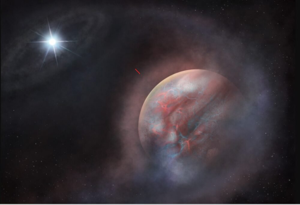
A planet orbiting once every 4 days around a white dwarf star HS 0209+0832 – about 270 light years in the direction of the constellation Pisces – is steadily losing its atmosphere to its host star. While many stars in solar systems beyond our own often feed on their planets, this particular star feeds on its own ashes.
The gaseous planet HS 0209+0832 b was discovered in 2024, when the Transiting Exoplanet Survey Satellite, a NASA space telescope, found it orbiting the white dwarf star over the course of four days. The new study followed through with detailed observations from TESS data, NASA’s space-based Far Ultraviolet Spectroscopic Explorer, in addition to the ESO’s mountain-based Very Large Telescope, to study the star’s atmosphere and in turn inferring some chemistry occurring in the planet.
In a study published in the journal Nature Astronomy on Monday and funded by NASA, European Research Council, Fundación Occident and the Instituto de Astrofísica de Canarias, an international team of astronomers have reported imprints of niobium, a heavy element, in the atmosphere of a white dwarf star.
Astronomers predict the transiting young planet around the dead star is supplying that niobium back to its host. The sighting is evidence of a “second generation” planet, one of many candidates identified over several years, manifesting in a myriad different ways from spent gas ejected in the wake of stellar deaths.
It adds to a known coterie of planets now found orbiting dead stars, astronomers are busy studying to spot signs of life.
What are white dwarf stars?
White dwarves are an exotic stars, and are all that’s left off giant stars shedding their large gaseous skin in violent deaths. Our sun is destined one day to transform into a white dwarf, but only after swelling in size some five billion years from now to become a red giant when it will eclipse past the earth’s orbit. It would take several million years after that for the red giant sun to shed its gaseous exterior to become a white dwarf.
Planets if any, found orbiting these dead stars may have likely migrated from the new solar system’s outer reaches. All that’s left off the progenitor star’s past are imprints of light metals and other elements on the white dwarf’s atmosphere. Such planets have previously been spotted orbiting pulsars, a kind of neutron star, back in 1992. In fact, its discovery had marked the first ever detection of any planet orbiting a star beyond our sun.
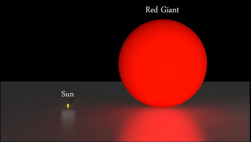
In five billion years, our sun will evolve to become a red giant star. Credit: Svitlana Leonidivna Malchenko
Sighting niobium
Elements such as niobium don’t typically form in the core of stars like our sun. Chemical production usually limits to elements lighter than or until iron, with its 26 protons and 30 neutrons. Beyond that, slamming an extra proton or neutron will cause those to split, leaving iron to be the last element to be directly forged.
Niobium, with 41 protons and 52 neutrons, is thought to be born after absorbing slow passing neutrons when the red giant star dies to form a white dwarf star. This niobium hitches a ride along with rest of the contents of the red giant star, farther into the outer reaches of the system after the formation of the white dwarf.
These contents could create a new disc of circumstellar material with dust and gas that could condense one day to form new planets. The “second generation” planet found orbiting the white dwarf star from the new study, could have been born this way.
Alternatively, it may have been a planet in the outskirts like Neptune, migrating inwards, and enriching itself with niobium-rich star material.
Either way, the planet got too close to its host star, which is irradiating its newfound niobium-rich atmosphere, stripping it away and devouring it.
While it’s likely not a candidate planet for life as we know it to be found, it’s discovery can help ascertain how such worlds are formed in the aftermath of a star’s various phases of evolution.


Climate Disasters Disrupted Schooling for 171 Million Students in 2025, UNICEF Finds

Brazil’s Amazon deforestation hits record low. Can the recovery last?

How Scientists Traced the Flow of Matter Around a Dead Star Using X-rays

India Scores Just 2 Out of 32 for Integrating Health into Climate Commitments

Global Job Market Faces a Growing Inclusion Gap as AI and Digitalisation Reshape Work

From Scams to Screens: How the National Stock Exchange Rewrote India’s Equity Story

Knowing When to Think for Ourselves: AI, Intuition and the Education of Discernment

After a Scorching Summer, Delhi’s Children Are Slow to Return Outdoors

Two Chemists Win Nobel Prize for Solving a Century-Old Puzzle: Why Life Picks One Hand Over the Other

Marshall Islands: Why the US Nuclear Legacy Is Back Before the UN

-

 Math3 months ago
The 2026 Fields Medals: Four Proofs, Four Decades-Old Problems Solved
-
EP Deep Dive: Data & Solutions3 months ago
After Kerala’s Deadliest Landslide, the Hardest Thing to Rebuild Was Childhood
-
EP Deep Dive: Data & Solutions4 months ago
West Asia Crisis: Can Kerala’s Returning Gulf Migrants Find a Future in the Green Economy?
-
Space & Physics5 months ago
India Semiconductor Mission: ‘It’s Not About Fabs. It’s About Building An Entire Ecosystem’
-
Interviews4 weeks ago
From Scams to Screens: How the National Stock Exchange Rewrote India’s Equity Story
-
Climate5 months ago
The Climate World Cup? How Climate Change Could Affect Player Performance at the 2026 World Cup
-
Society3 months ago
What Is Civilisational Diplomacy? Understanding India’s Newest Foreign Policy Tool
-
Society4 months ago
From Bell Labs to the Classroom: A Second Career in Teaching