Space & Physics
The various avatars of the Hall effect
In this second article of Ed Publica’s series on the Hall effect, Dr. Saraubh Basu examines the physics of the Hall effect variants discovered over the course of the past century.

This is the second article of Ed Publica’s series on the Hall effect, which covers the various manifestations of the Hall effect. You can read the first article here.
The ‘anomalous’ Hall effect
In 1881, just two years after Edwin Hall discovered the eponymous Hall effect, he spotted an anomaly when replicating the effect with ferromagnets.
He had observed a tenfold deflection of electric charges this time around, compared to non-magnetic conductors.
Suspecting the magnetic properties played a role, this avatar of the Hall effect is dubbed the anomalous Hall effect. The word ‘anomalous’ is used owing to the fact that external magnetic field no longer remains as a stringent requirement for the Hall effect; instead, the intrinsic magnetization (for instance, the ferromagnet in the above example) fulfils that criterion.
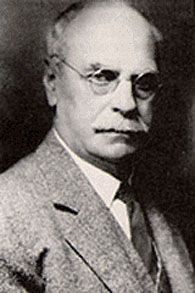
The physicist Edwin Hall. Credit: Wikimedia
The Hall resistivity in ferromagnets increase steeply under the presence of very weak magnetic fields. However, in stronger magnetic fields, the Hall resistivity doesn’t increase further very much. This saturation is rather strange, for it is in contrast to the classical Hall effect where the Hall resistivity maintains its steady growth.
There are several other effects that play a crucial role in determining the anomalous Hall resistivity, thus making it a complicated phenomenon that physicists lack comprehensive understanding about, in comparison to the various other avatars of the Hall effect.
Quantum avatar(s)
The fact that a simple lab experiment showed how the Hall resistivity can be expressed as an equation that contains merely constants, opened up a a plethora of research to understand the cause of this ‘universality’. For it hinted to the involvement of a very fundamental phenomenon.
In 1980, Klaus von Klitzing discovered the quantum avatar of the Hall effect was detected. He was amidst research at a magnetic facility in Grenoble, France, working to improve electron mobility in metal oxide semiconductor field effect transistors (MOSFET). These are transistors that typically operate at extremely low temperatures and under intense magnetic fields.
von Klitzing observed his sample’s Hall resistivity assuming discretized values. This means the resistivity jumps in steps, by a fixed amount that can be scaled as multiples of an integer number (includes 0 along with whole numbers such as 1,2,3, and so on). This discretization reveals the underlying quantum mechanical behavior that has been unraveled at long last – thus bearing its name – the integer quantum Hall effect. von Klitzing later won the Nobel Prize in Physics for 1985 for this work.
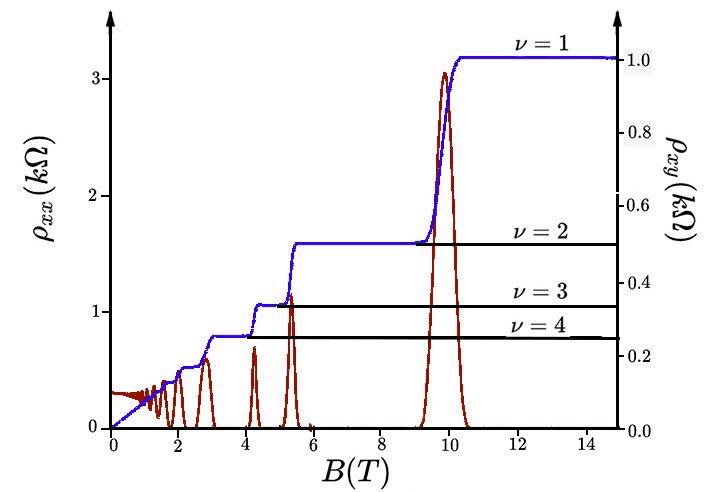
The plot here depicts the transverse and longitudinal Hall resistivity (y-axis) increasing in integer steps as the magnetic field (x-axis) increases. This is due to the integer quantum Hall effect. Credit: Wikimedia
But the quantization isn’t limited to integer multiples. In fact, two years later, the fractional quantum Hall effect was observed in experiments. It was shown there were about 100 fractions, including those that aren’t whole numbers that were now in the formula.
Robert Laughlin, who would later win a share of the 1998 Nobel Prize in Physics, proposed a theory to explain the observations. It boils down to the interaction among electrons, either due to the Coulombic repulsion force or the Pauli exclusion principle.
These interacts would eventually split the degeneracy of these enormously degenerate Landau energy levels. These are quantum states occupied by electrons that complete circular revolutions under the influence of an external magnetic field. Splitting these degeneracies, lead to the opening of an energy gap, for the fractional quantum Hall effect to be observed.
‘Spin’ avatar(s)
Just as there are electric charges in nature, so are there spin currents found in nature. ‘Spin’ is a key property found in quantum particles. Unlike what the name suggests, these quantum particles don’t spin or rotate about any axis passing through them. However, these particles carry an angular momentum as though it does spin.
In 1971, before von Klitzing observed the quantum Hall effect, Mikhail Dyakonov and Vladimir Perel hypothesized the spin Hall effect.
In this avatar of the Hall effect, quantum spins of opposite kinds accumulate at the edges of the sample, orthogonal to the direction in which the charge current passes.
The spin selection can be facilitated by the spin-orbit coupling. This refers to the modified energy levels in an atom when the electron’s motion is under the influence on the magnetic field generated by the nucleus. Strong coupling may be intrinsic to doped semiconductors. The proposal has triggered intense investigation of the phenomenon, with first experimental observations of the spin Hall effect seen in n-doped semiconductors and two-dimensional hole gases.
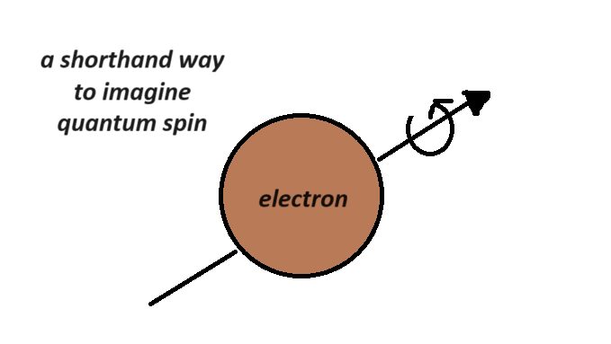
Quantum spins don’t really look like the depiction above, which is meant to showcase a fact that particles like electrons do have an intrinsic angular momentum nonetheless. Credit: Karthik / Ed Publica
For more than a decade, studies concerning the spin current and its application to novel spintronics (or spin electronics) have received plethora of attention. This is with regard to efficiently generating, manipulating and detecting spin accumulation in a sample material. Some progress has also occurred from the device fabrication perspective via techniques such as spin injection, among others.
A major advantage in dealing with the spin current lies in the non-dissipative (or very less dissipation) nature which arises owing to the time reversal invariance of the spin current. This presents a non-dissipative scenario (unlike the dissipative effects seen with charged currents), thus making it quite advantageous for spin transport phenomena.
Furthermore, a quantized version of the spin Hall effect exists, with mercury telluride and cadmium telluride quantum well superlattices, showcasing this effect. In 2005, a quantum treatment was proposed by Charles Kane and Eugene Mele, in the form of a tight binding toy model of electrons operating in a two-dimensional honeycomb lattice.
In fact, the ‘wonder material’ graphene, which is a two-dimensional honeycomb lattice constituting carbon atoms, does satisfy some key requirements for the quantum spin Hall effect. However, it lacks a large spin-orbit coupling among other requirements.
Nonetheless, graphene’s ability to entertain the quantum spin Hall effect, makes it a prospective candidate to find applications in next-generation spintronic devices.











Space & Physics
India’s New Satellite Will Be Tested During Disasters
India’s latest Earth-observation satellite, EOS-05, could give disaster agencies a broader and more frequent view of floods, landslides and other hazards. But its real value will depend on how quickly satellite data can be turned into information that helps authorities act on the ground.

Space & Physics
India’s Moonshot Moment: Can New Delhi Turn Orbit Into Influence
India’s space mission is entering a new era, from Gaganyaan and space stations to private startups, space diplomacy and national security.


Gaganyaan is only the beginning. India’s space mission faces new opportunities and challenges as human spaceflight, diplomacy, private industry and security reshape its ambitions beyond Earth.
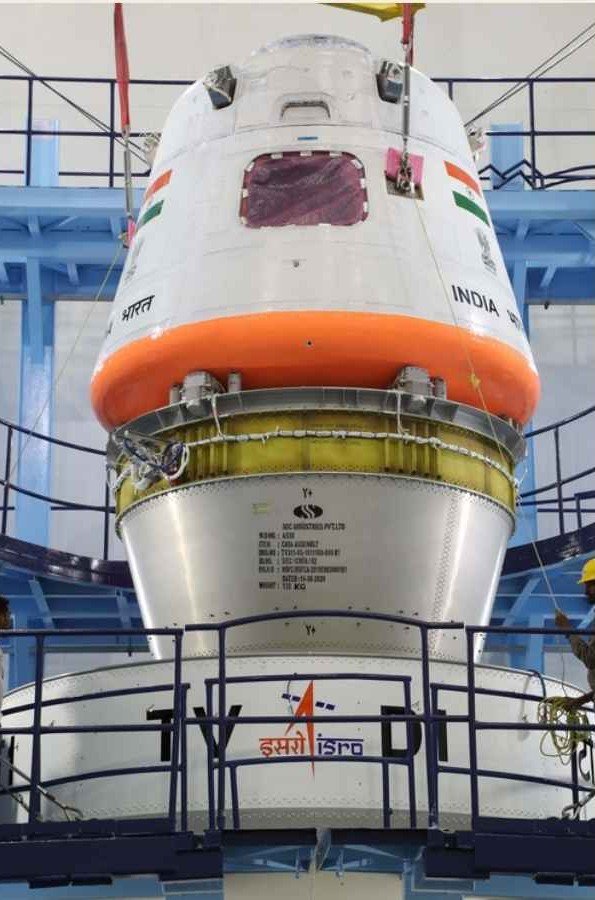
Indian human space programme Gaganyaan is mooted by Indian Space Research Organisation. This ambitious space mission aims to send Indian astronauts in Outer Space indigenously by the proactive leadership of the Indian government. India as a leading space power of the world aims to demonstrate her space capabilities and research in the final frontier. The Gaganyaan mission is the dream of 1.4 billion Indians. The programme will be initiated in 2027 creating a historic mark in the collective space exploration journeys. This is a stepping stone as NASA is envisioning to make Moon as the next base for active space programmes by 2030.
According to NASA this spectacular feat will be achieved soon within 3 years. NASA has asked India’s ISRO to join for the permanent Lunar base in the south pole of Moon. Here comes the significance of Indo-US space partnership and how India will navigate through the space diplomacy keeping in mind of Indian dream of Bharatiya Antariksh Station and the long lasting commitment to strategic autonomy and an independent foreign policy. India already signed the Artemis accords in June 2023. If India is ready to be part of this initiative, it will mark the beginning of a new era in India-United States space cooperation. The question is how India will navigate this process, protecting its sovereignty and national interest while engaging with NASA to help build a new civilisation of space travellers on the lunar surface. According to media reports India’s spectacular success with the Chandrayaan missions has led the United States to choose India as a natural partner, inviting it to join space exploration programmes on the Moon.
India’s Space Mission: The Next Frontier of Global Power
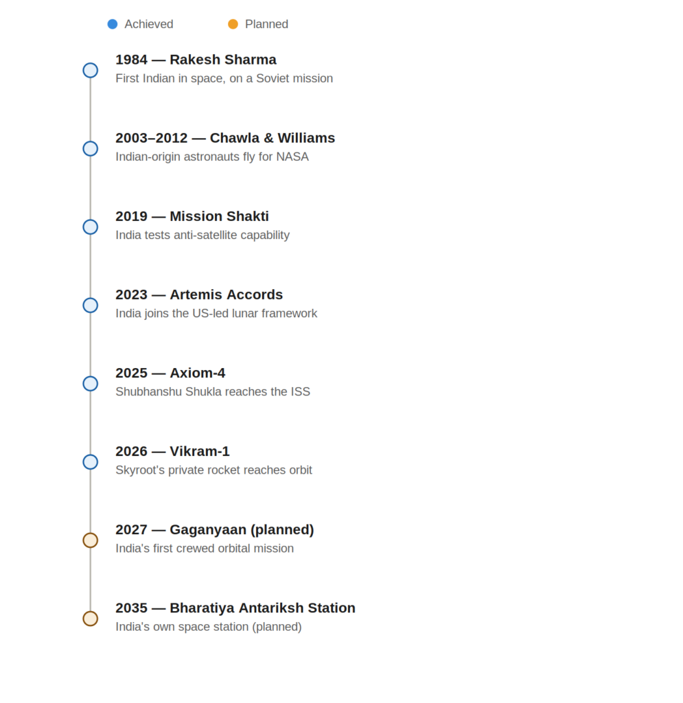
The Gaganyaan mission is significant for strengthening Indian space station’s vision. The Bharatiya Antariksh Station is an Indian space station which is a symbol of Indian space nationalism and a centre for joint research with friendly nations. India is actively pushing for space diplomacy and it is evident from the trainings received by Gaganyaan crew members. They have trained in Russia and the United States, continuing India’s commitment to strong bilateral ties with both Cold War-era rivals. Space exploration and travel are combined with diplomacy, as Indian foreign policy in a multipolar world order pushes for strong partnerships with both Russia and the United States.
Indian Air Force veteran Wing Commander Rakesh Sharma was the first Indian cosmonaut to reach the final frontier, in a Soviet space mission. Following this historic feat, Kalpana Chawla and Sunita Williams travelled to outer space on American missions. Recently, Group Captain Shubhanshu Shukla represented India in the Axiom mission successfully travelling to International Space Station and returned safely as a national hero. He is also part of the Gaganyaan mission. Colonel Anil Menon, who is part of the US Space Force, is also now in outer space. He has strong Indian connections, making him the first astronaut with roots in Kerala to explore the domain of outer space.
With privatisation in outer space in India, Skyroot Aerospace, a private company based in Hyderabad, successfully launched Vikram-1 rocket to low Earth orbit. Thus India is taking leverage of the infinite possibilities chasing stars and galaxies. Indian space ambitions are at a historic juncture now, with over 400 private Space startups. Another mission is aiming for a reusable re-entry vehicle, targeted for launch in 2027, building on ISRO’s success with the Pushpak mission, the Reusable Launch Vehicle Landing Experiment, in 2024.
However, there are concerns in India’s space sector, with many ISRO scientists seeking early retirement. The efficiency of major projects like Aditya and Gaganyaan should not be affected by this. Former ISRO Chairman G Madhavan Nair shared his concerns with the media about bureaucratisation within the organisation. ISRO is a symbol of India’s space story which is filled with resilience and strength of great visionary leaders like Dr Vikram Sarabhai and Dr APJ Abdul Kalam. Unfortunately, there have been budgetary cuts to major ISRO space projects. The government’s focus on Viksit Bharat, a holistically developed India, is only possible with investment in science and technology, and in-depth research in the domain of outer space.
Outer space is militarised, and the race for resource nationalism is a reality. For India to emerge as a global power, investment in space exploration is inevitable. Nations are increasingly aware of the strategic use of outer space for securing national interests. Satellites with civilian and national security purposes are critical assets of any nation. India too has many civilian and strategic assets in outer space, and protecting these is the responsibility of the government. The anti-satellite test Mission Shakti is a milestone demonstrating India’s hard-power capabilities in outer space. Some nations have capabilities such as laser-guided weapons, which can disable or destroy an enemy’s assets during conflict. Space is a key domain for ensuring seamless communication and intelligence-sharing during both war and peace.
Intelligence and surveillance are key factors in winning the wars of the present and future. The dominance in space technology and information superiority will determine the victories of nations fighting for their national interest.
In India, the share of higher education in the annual budgetary allocation remains low. A young generation passionate to explore arenas of space science is to be inculcated with the right mindset. Allocation of funds in education sector is a key requirement for building a strong India with educated and skilled youth. ISRO’s active collaboration with 100 Atal Tinkering Labs is a positive step in inculcating the spirit of scientific enquiry at the grassroots level. Support and encouragement for students in the creative arts and sciences is the need of the hour. Atal Tinkering Labs and India’s startup ecosystem can achieve greater synergy, ensuring a seamless transition from school life to entrepreneurship, from plan to execution.
Human activity has actively degraded the ecosystem, impacting life on both land and water. Now, with active competition in the arena of outer space, space debris is a serious global security challenge. This debris travels swiftly in outer space, damaging active space assets including civilian and defence satellites. The young budding scientists of India need to re-invent and discover practical solutions to the pressing global challenge of space debris and work with relentless passion for making a strong and stable India.
Space & Physics
Meteorite Dust Reveals Evidence of Magnetic Field in the Young Solar System
A magnetic field in the early solar system has been detected in ancient meteorite grains, offering evidence that magnetism helped shape the young sun.


KSBB Workshop Examines Biodiversity, Climate and Environmental Reporting

Why Global Tech and Industry Lean on Indian Talent

From Silicon Valley to Sustainable Period Care; How This Engineer Is Rethinking Menstruation with Science

India tops the world for population exposed to climate-driven risky heat

Can a Webcam Replace the Guru? A Kerala Startup Is Betting Yes

Farmers Borrowed to Build ‘Diggis’. Two Years Later, They Are Still Waiting for the Subsidy

Our Algorithm Knows What We Want Before We Do. That is the Problem.

When Decarbonisation Becomes the Real Conversation at Tiruppur’s Knit Show

When the Himalayas Collapse Without Warning, What Counts as Preparedness?

The Engineer of Tomorrow Is Already Here
-

 Math2 months ago
The 2026 Fields Medals: Four Proofs, Four Decades-Old Problems Solved
-
Climate2 months ago
After Kerala’s Deadliest Landslide, the Hardest Thing to Rebuild Was Childhood
-
Society2 months ago
West Asia Crisis: Can Kerala’s Returning Gulf Migrants Find a Future in the Green Economy?
-
Space & Physics4 months ago
India Semiconductor Mission: ‘It’s Not About Fabs. It’s About Building An Entire Ecosystem’
-
Climate4 months ago
The Climate World Cup? How Climate Change Could Affect Player Performance at the 2026 World Cup
-
Society2 months ago
What Is Civilisational Diplomacy? Understanding India’s Newest Foreign Policy Tool
-
Society3 months ago
From Bell Labs to the Classroom: A Second Career in Teaching
-
Space & Physics4 months ago
Engineers Develop Dual-Mode Propulsion System for Next-Generation Small Satellites