Space & Physics
New antenna design could help detect faint cosmological signals
This could revolutionise our ability to detect the faint signals of Cosmological Recombination Radiation (CRR)

In an intriguing development, scientists at the Raman Research Institute (RRI) in Bangalore, India, have developed a novel antenna design that could revolutionise our ability to detect the faint signals of Cosmological Recombination Radiation (CRR).
These signals, which are crucial for understanding the thermal and ionization history of the Universe, have so far remained undetected due to their elusive nature. The newly designed antenna is capable of measuring signals in the 2.5 to 4 Gigahertz (GHz) frequency range, which is optimal for detecting CRR, a signal that is approximately one billion times fainter than the Cosmic Microwave Background (CMB).
As per available sources, the universe is approximately 13.8 billion years old, and in its earliest stages, it was extremely hot and dense. During this time, the Universe was composed of a plasma of free electrons, protons, and light nuclei such as helium and lithium. The radiation coexisting with this matter has been detected today as the CMB, which holds vital information about the early cosmological and astrophysical processes.
One such process, known as the Epoch of Recombination, marks the transition from a fully ionized primordial plasma to mostly neutral hydrogen and helium atoms. This transition emitted photons, creating the Cosmological Recombination Radiation (CRR), which distorts the underlying CMB spectrum. Detecting these faint CRR signals would provide a wealth of information about the Universe’s early ionization and thermal history and could even offer the first experimental measurements of helium abundance before it was synthesized in the cores of stars.
However, detecting CRR is a significant challenge because these signals are extremely weak—about nine orders of magnitude fainter than the CMB. To address this, scientists need highly sensitive instruments that can isolate these signals from the vast cosmic noise surrounding them.
To this end, researchers from RRI, including Mayuri Rao and Keerthipriya Sathish, along with Debdeep Sarkar from the Indian Institute of Science (IISc), have developed an innovative ground-based broadband antenna designed to detect signals as faint as one part in 10,000. Their design is capable of making sky measurements in the 2.5 to 4 GHz range, the frequency band most suitable for CRR detection.
According to Keerthipriya Sathish, the lead author of the study, “For the sky measurements we plan to perform, this broadband antenna offers the highest sensitivity compared to other antennas designed for the same bandwidth. The antenna’s frequency-independent performance across a wide range and its smooth frequency response are features that set it apart from conventional designs.”
The antenna is compact and lightweight, weighing just 150 grams, with a square shape measuring 14 cm by 14 cm.
The proposed antenna is a dual-polarized dipole antenna with a unique four-arm structure shaped like a fantail. This design ensures that the antenna maintains the same radiation pattern across its entire operational bandwidth, with a mere 1% variation in its characteristics. This is crucial for distinguishing spectral distortions from galactic foregrounds. The antenna’s custom design allows it to “stare” at the same patch of sky throughout its full operational range of 1.5 GHz (from 2.5 to 4 GHz), which is key to separating the CRR signals from other cosmic noise.
The antenna is compact and lightweight, weighing just 150 grams, with a square shape measuring 14 cm by 14 cm. It is made using a low-loss dielectric flat substrate on which the antenna is etched in copper, while the bottom features an aluminum ground plate. Between these plates lies a radio-transparent foam layer that houses the antenna’s connectors and receiver base.
With a sensitivity of around 30 millikelvin (mK) across the 2.5-4 GHz frequency range, the antenna is capable of detecting tiny temperature variations in the sky. Even before being scaled to a full array, this antenna design is expected to provide valuable first scientific results when integrated with a custom receiver. One of the anticipated experiments is to study an excess radiation reported at 3.3 GHz, which has been speculated to result from exotic phenomena, including dark matter annihilation. These early tests will help refine the antenna’s performance and guide future design improvements aimed at achieving the sensitivity required for CRR detection.
The researchers plan to deploy an array of these antennas in radio-quiet areas, where radio frequency interference is minimal or absent. The antenna’s design is straightforward and can be easily fabricated using methods similar to those employed in Printed Circuit Board (PCB) manufacturing, ensuring high machining accuracy and consistency for scaling up to multiple-element arrays. The antenna is portable, making it easy to deploy in remote locations for scientific observations.
The team is already looking ahead, planning further improvements to achieve even greater sensitivity, with a long-term goal of detecting CRR signals at sensitivities as low as one part per billion. With this innovative antenna design, the team hopes to make significant strides toward uncovering the secrets of the early Universe and its formation.
Space & Physics
Researchers Develop Ultra-Efficient Chip for Post-Quantum Security in Medical Devices
The breakthrough addresses a critical vulnerability in next-generation healthcare technology as quantum computing advances threaten current encryption standards.
Breakthrough Enables Strong Encryption on Tiny, Power-Constrained Devices
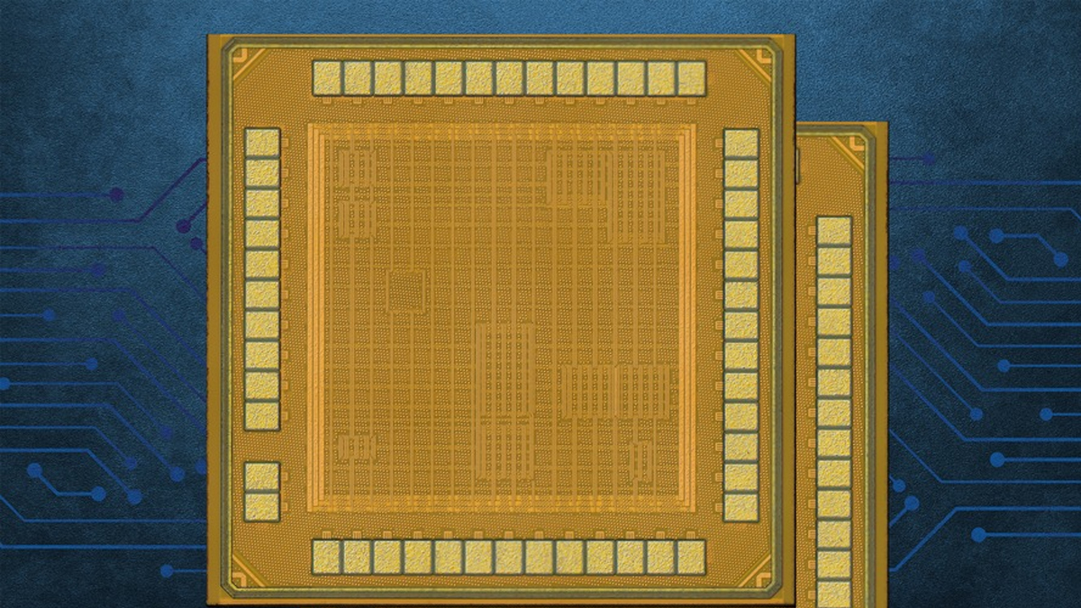
Researchers at the Massachusetts Institute of Technology have developed a highly energy-efficient microchip capable of running advanced post-quantum cryptography (PQC) on small, power-limited devices such as pacemakers, insulin pumps, and ingestible sensors. The breakthrough addresses a critical vulnerability in next-generation healthcare technology as quantum computing advances threaten current encryption standards.
The chip, roughly the size of a needle tip, integrates robust security features designed to protect sensitive patient data while maintaining extremely low power consumption. This makes it suitable for wireless biomedical devices that have historically lacked strong encryption due to energy constraints.
Why Post-Quantum Cryptography Matters
As quantum computers evolve, traditional encryption methods are expected to become obsolete. Governments and regulatory bodies, including the National Institute of Standards and Technology (NIST), are already preparing to transition toward PQC algorithms to safeguard digital infrastructure.
However, PQC techniques are computationally intensive, often increasing energy usage by up to 100–1000 times—making them impractical for small, battery-powered devices until now.
This new chip bridges that gap by enabling advanced encryption without significantly increasing energy demand.
Key Innovations Behind the Chip
Multi-Layered Security Design
The chip incorporates multiple PQC algorithms to ensure long-term resilience, even if one encryption method becomes vulnerable in the future.
Built-in Random Number Generator
A highly efficient on-chip random number generator strengthens encryption by producing secure cryptographic keys internally, eliminating reliance on external components.
Protection Against Physical Attacks
The design includes safeguards against “power side-channel attacks,” where hackers attempt to extract data by analyzing power consumption patterns.
Early Fault Detection
The chip can detect voltage irregularities and abort compromised operations early, preventing energy waste and potential security breaches.
Major Gains in Energy Efficiency
The researchers report that the chip achieves 20 to 60 times greater energy efficiency compared to existing PQC implementations, while also occupying a smaller physical footprint.
This efficiency breakthrough is crucial for expanding secure computing to edge devices—systems that operate outside traditional data centers, often with strict power limitations.
Space & Physics
The Universe Is Ringing
How gravitational waves from colliding black holes are opening an entirely new way of exploring the cosmos
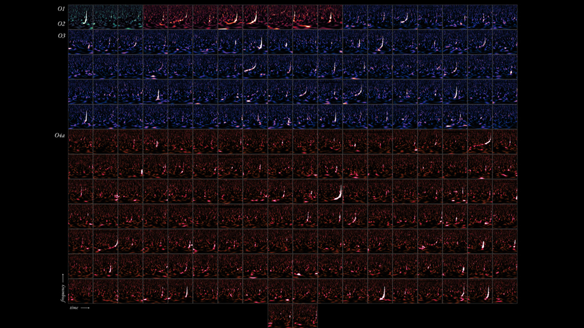
More than a century after Albert Einstein predicted them, gravitational waves are transforming astronomy. Ripples in space-time produced by colliding black holes and neutron stars are now being detected routinely, revealing a universe filled with violent mergers and cosmic echoes that have travelled billions of years to reach Earth.
A Ripple Across the Cosmos
When the densest objects in the universe collide, the impact does not simply end with the destruction or merger of stars. It sends ripples through the very fabric of space and time.
These ripples—known as gravitational waves—spread outward at the speed of light, crossing galaxies and cosmic voids for millions or even billions of years. By the time they reach Earth, they are unimaginably faint distortions of space itself.
Yet scientists have learned how to detect them.

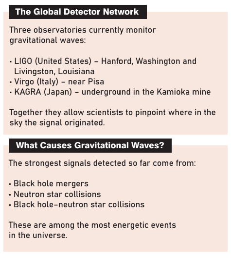
A global network of observatories now monitors these tiny disturbances: the Laser Interferometer Gravitational-Wave Observatory (LIGO) in the United States, the Virgo detector in Italy, and the Kamioka Gravitational Wave Detector (KAGRA) in Japan. Together, these instruments form one of the most sensitive scientific experiments ever constructed, capable of detecting distortions smaller than the width of a proton.
Through them, astronomers have begun to “listen” to the universe.
And what they are hearing is astonishing.
A Universe Filled with Collisions
The LIGO–Virgo–KAGRA (LVK) Collaboration has now released the latest compilation of gravitational-wave detections, to appear in a special issue of Astrophysical Journal Letters. The findings suggest that the cosmos is reverberating with collisions far more frequently than scientists once imagined.
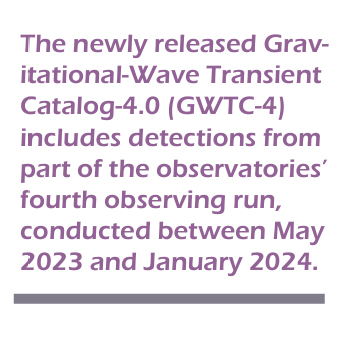
The newly released Gravitational-Wave Transient Catalog-4.0 (GWTC-4) includes detections from part of the observatories’ fourth observing run, conducted between May 2023 and January 2024.

In just nine months, the detectors recorded 128 new gravitational-wave candidates—signals that likely originated from extreme astrophysical events occurring hundreds of millions or billions of light-years away.
This newest batch more than doubles the size of the gravitational-wave catalog, which previously contained 90 candidates from earlier observing runs.
“The beautiful science that we are able to do with this catalog is enabled by significant improvements in the sensitivity of the gravitational-wave detectors as well as more powerful analysis techniques,” says Nergis Mavalvala, a member of the LVK collaboration and dean of the MIT School of Science.

What began in 2015 with the first historic detection has now become a steady stream of discoveries.
“In the past decade, gravitational wave astronomy has progressed from the first detection to the observation of hundreds of black hole mergers,” says Stephen Fairhurst, professor at Cardiff University and spokesperson for the LIGO Scientific Collaboration. “These observations enable us to better understand how black holes form from the collapse of massive stars, probe the cosmological evolution of the universe and provide increasingly rigorous confirmations of the theory of general relativity.”
When Black Holes Dance
Most gravitational waves detected so far originate from binary black holes—pairs of black holes locked in orbit around each other.
Over time, gravity draws them closer together. As they spiral inward, they release enormous amounts of energy in the form of gravitational waves. In the final fraction of a second, the two objects merge in a titanic collision, forming a single, larger black hole.
These cosmic dances are among the most energetic events in the universe.
Black holes themselves are born when massive stars collapse at the end of their lives, compressing enormous amounts of matter into regions so dense that not even light can escape.
Many form in pairs. When they eventually collide, the event sends gravitational waves surging through space.
The first such detection, announced in 2016, confirmed a century-old prediction of Einstein’s theory of general relativity. Since then, dozens—and now hundreds—of similar events have been observed.
But the latest catalog shows that the universe is far more diverse than scientists once believed.
Pushing the Edges of Black Hole Physics
The newly detected signals reveal a remarkable variety of cosmic systems.
Among them are the heaviest black hole binaries ever detected, systems where the masses of the two black holes are strikingly unequal, and pairs spinning at astonishing speeds.
“The message from this catalog is: We are expanding into new parts of what we call ‘parameter space’ and a whole new variety of black holes,” says Daniel Williams, a research fellow at the University of Glasgow. “We are really pushing the edges, and are seeing things that are more massive, spinning faster, and are more astrophysically interesting and unusual.”

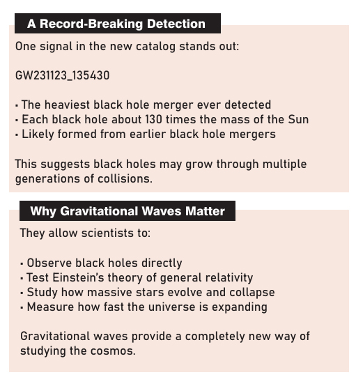
One particularly dramatic signal—GW231123_135430—appears to have originated from two enormous black holes, each roughly 130 times the mass of the Sun. Most previously observed mergers involved black holes closer to 30 solar masses.
The extraordinary size of these objects suggests they may themselves have formed from earlier black hole mergers—a kind of cosmic generational chain.
Another remarkable event, GW231028_153006, revealed a binary in which both black holes are spinning at around 40 percent of the speed of light.
And in GW231118_005626, scientists detected an unusually uneven pair where one black hole is roughly twice as massive as the other.
“One of the striking things about our collection of black holes is their broad range of properties,” says Jack Heinzel, an MIT graduate student who contributed to the catalog’s analysis. “Some of them are over 100 times the mass of our sun, others are as small as only a few times the mass of the sun. Some black holes are rapidly spinning, others have no measurable spin.”
“We still don’t completely understand how black holes form in the universe,” he adds, “but our observations offer a crucial insight into these questions.”
Catching a Whisper in Space-Time
Detecting gravitational waves requires extraordinary precision.
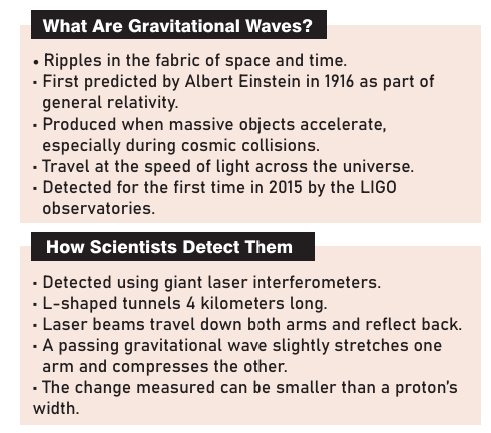
The observatories use L-shaped interferometers with arms several kilometers long. Laser beams travel down these tunnels and reflect back to their source.
If a gravitational wave passes through the detector, it slightly stretches one arm while compressing the other, changing the distance the light travels by an incredibly tiny amount.
These changes can be smaller than one-thousandth the diameter of a proton.
Even with such advanced technology, detections remain unpredictable.

“You can’t ever predict when a gravitational wave is going to come into your detector,” says Amanda Baylor, a graduate student at the University of Wisconsin–Milwaukee who worked on the signal search. “We could have five detections in one day, or one detection every 20 days. The universe is just so random.”
Recent upgrades have dramatically improved the detectors’ reach. LIGO can now detect signals from neutron star collisions up to one billion light-years away, and black hole mergers far beyond that.
Testing Einstein’s Ultimate Theory
Gravitational waves are not only revealing spectacular cosmic events. They are also providing some of the most extreme tests ever conducted of Einstein’s theory of general relativity.
Black holes themselves are one of the most extraordinary predictions of the theory.
“Black holes are one of the most iconic and mind-bending predictions of general relativity,” says Aaron Zimmerman, associate professor of physics at the University of Texas at Austin.
When two black holes collide, he explains, they “shake up space and time more intensely than almost any other process we can imagine observing.”
One particularly powerful signal—GW230814_230901—allowed scientists to analyze the structure of the gravitational wave in exceptional detail.
“So far, the theory is passing all our tests,” Zimmerman says. “But we’re also learning that we have to make even more accurate predictions to keep up with all the data the universe is giving us.”
Measuring the Expansion of the Universe
Gravitational waves are also becoming powerful tools for answering one of cosmology’s biggest questions: how fast the universe is expanding.
Astronomers measure this expansion using the Hubble constant, but different methods have produced conflicting results.
Gravitational waves offer an independent approach.
“Merging black holes have a really unique property: We can tell how far away they are from Earth just from analyzing their signals,” says Rachel Gray, a lecturer at the University of Glasgow.
“So, every merging black hole gives us a measurement of the Hubble constant, and by combining all of the gravitational wave sources together, we can vastly improve how accurate this measurement is.”
Using the current gravitational-wave catalog, scientists estimate that the universe is expanding at roughly 76 kilometers per second per megaparsec.
For now, the uncertainty remains large—but future detections could sharpen the measurement significantly.

Listening to the Future
Only a decade ago, gravitational waves were purely theoretical signals.
Today, they are transforming astronomy.
With every new detection, scientists gain another glimpse into the hidden life of the universe: the birth of black holes, the evolution of galaxies, and the behavior of gravity under the most extreme conditions imaginable.
“Each new gravitational-wave detection allows us to unlock another piece of the universe’s puzzle in ways we couldn’t just a decade ago,” says Lucy Thomas, a postdoctoral researcher at the Caltech LIGO Lab.
“It’s incredibly exciting to think about what astrophysical mysteries and surprises we can uncover with future observing runs.”
The instruments on Earth are quiet, their lasers moving silently down vacuum tunnels. But far beyond our galaxy, black holes continue to collide.
And with each collision, the universe sends out another ripple—another echo across the cosmos—waiting for us to hear it.
Space & Physics
NASA’s Artemis II Captures Stunning ‘Earthset’ Over the Moon
NASA’s Artemis II crew captures a rare Earthset over the Moon, revealing lunar basins, craters, and Earth’s night-day divide.

NASA’s Artemis II mission has captured a striking new perspective of the Moon, showing Earth setting beyond the lunar horizon in a rare and visually dramatic moment from deep space.
The image, taken on April 6, 2026, at 6:41 p.m. EDT by the Artemis II crew during their journey around the far side of the Moon, reveals Earth partially dipping behind the Moon’s curved limb—an event often described as an “Earthset.”

A Geological Snapshot of the Moon
Beyond its visual impact, the image offers a detailed look at the Moon’s complex surface.
The Orientale basin, one of the Moon’s most prominent impact structures, is visible along the edge of the lunar surface. Nearby, the Hertzsprung Basin appears as faint concentric rings, partially disrupted by the younger Vavilov crater, which sits atop the older geological formation.
Also visible are chains of secondary craters—linear indentations formed by debris ejected during the massive impact that created the Orientale basin.

Artemis II: Earth in Shadow and Light
The photograph also captures Earth in a moment of contrast.
The darkened portion of the planet is in nighttime, while the illuminated side reveals swirling cloud formations over Australia and the Oceania region, offering a reminder of Earth’s dynamic atmosphere even from hundreds of thousands of kilometres away.
Artemis II: A New Era of Lunar Exploration
The Artemis II mission marks a major step in NASA’s return to the Moon, carrying astronauts on a crewed journey around the lunar surface for the first time in over five decades.
Images like this not only provide scientific insights into lunar geology but also offer a powerful visual connection between Earth and its nearest celestial neighbour—highlighting both the scale of space exploration and the fragility of our home planet.

-

 Society4 months ago
The Ten-Rupee Doctor Who Sparked a Health Revolution in Kerala’s Tribal Highlands
-

 Society4 months ago
From Qubits to Folk Puppetry: India’s Biggest Quantum Science Communication Conclave Wraps Up in Ahmedabad
-

 COP306 months ago
Brazil Cuts Emissions by 17% in 2024—Biggest Drop in 16 Years, Yet Paris Target Out of Reach
-

 Earth6 months ago
Data Becomes the New Oil: IEA Says AI Boom Driving Global Power Demand
-

 COP305 months ago
Corporate Capture: Fossil Fuel Lobbyists at COP30 Hit Record High, Outnumbering Delegates from Climate-Vulnerable Nations
-

 Space & Physics4 months ago
Indian Physicists Win 2025 ICTP Prize for Breakthroughs in Quantum Many-Body Physics
-

 Health6 months ago
Air Pollution Claimed 1.7 Million Indian Lives and 9.5% of GDP, Finds The Lancet
-

 Sustainable Energy5 months ago
The $76/MWh Breakthrough: Battery-Backed Solar Becomes the Cheapest Firm Power


