Space & Physics
India’s space economy soars: A $130 million VC fund to ignite innovation
The $130 million Venture Capital Fund is more than just a financial investment; it’s a catalyst for growth, innovation, and self-reliance in India’s space sector

In a dynamic leap toward becoming a global leader in space technology, India is set to launch a $130 million Venture Capital (VC) Fund dedicated to its burgeoning space sector. Announced by Prime Minister Narendra Modi, this initiative, spearheaded by the Indian National Space Promotion and Authorization Centre (IN-SPACe), aims to ignite innovation and support the country’s growing number of space startups.
A New Era for Space Startups
For many aspiring entrepreneurs in India’s space industry, access to funding has often been a significant barrier. Traditional lenders are typically hesitant to invest in the high-risk, high-reward arena of space technology. This new VC Fund is designed to fill that gap, providing essential capital to startups looking to take off.
“The fund is a game-changer,” says Dr. Anjali Rao, a space technology analyst. “It signals to investors that the government believes in the potential of our space industry. We’re going to see a surge in innovative solutions coming from Indian startups.”
Bridging the Funding Gap
The $130 million crore initiative is not just about money; it’s about fostering a supportive ecosystem. Over the next five years, the fund will allocate capital strategically, with plans to invest between $18.3 million and $30.5 million annually. This structured investment approach is designed to cater to both early-stage startups and more established firms, ensuring that companies at various levels of maturity can benefit.
For startups in their infancy, funding will range from $1.22 million to $ 3.66 million. More established companies with proven track records could receive up to $7.32 million. This tiered approach allows us to support a diverse range of companies and their unique needs.
Talent Retention and Economic Growth
One of the critical goals of the VC Fund is to prevent brain drain. Many skilled professionals have moved abroad for better opportunities, but this fund aims to retain talent by creating a thriving domestic ecosystem. “We’re not just creating jobs; we’re building a community of innovators who want to stay and grow in India,” says Dr. Meera Gupta, a startup consultant based in Mumbai, India.
Currently, India’s space economy is valued at approximately USD 8.4 billion, capturing about 2% of the global market. The government aims to quintuple this figure to USD 44 billion by 2033
The anticipated impact on employment is significant. The fund is expected to generate thousands of jobs across various sectors, from engineering to data analysis. As companies expand, indirect job creation in logistics and support services will also flourish.
Global Ambitions
Currently, India’s space economy is valued at approximately USD 8.4 billion, capturing about 2% of the global market. The government aims to quintuple this figure to USD 44 billion by 2033, with a strong focus on increasing exports. This vision positions India as a formidable player in the international space arena.
For startups in their infancy, funding will range from $1.22 million to $ 3.66 million. More established companies with proven track records could receive up to $7.32 million
As countries around the world recognize the strategic importance of their space sectors, India’s initiative aligns with global trends. Countries like the UK, Italy, and Japan have established similar funds to stimulate innovation and private sector participation. “India is taking a bold step in this direction, and the potential is immense,” remarks Dr. Rao.
Looking Ahead
As the launch of the VC Fund approaches, excitement is building within the Indian space community. Startups are already gearing up to apply for funding, eager to leverage the support that will help them bring their visions to life. “This is just the beginning,” says Dr. Gupta. “With the right backing, we can achieve remarkable things.”
The $130 million Venture Capital Fund is more than just a financial investment; it’s a catalyst for growth, innovation, and self-reliance in India’s space sector. As India looks to the stars, the world will be watching to see how this initiative transforms the landscape of space technology.


Space & Physics
Nobel Prize in Physics: Clarke, Devoret, and Martinis Honoured for Pioneering Quantum Discoveries
The 2025 Nobel Prize in Physics honours John Clarke, Michel H. Devoret, and John M. Martinis for revealing how entire electrical circuits can display quantum behaviour — a discovery that paved the way for modern quantum computing.

The 2025 Nobel Prize in Physics has been awarded to John Clarke, Michel H. Devoret, and John M. Martinis for their landmark discovery of macroscopic quantum mechanical tunnelling and energy quantisation in an electric circuit, an innovation that laid the foundation for today’s quantum computing revolution.
Announcing the prize, Olle Eriksson, Chair of the Nobel Committee for Physics, said, “It is wonderful to be able to celebrate the way that century-old quantum mechanics continually offers new surprises. It is also enormously useful, as quantum mechanics is the foundation of all digital technology.”
The Committee described their discovery as a “turning point in understanding how quantum mechanics manifests at the macroscopic scale,” bridging the gap between classical electronics and quantum physics.
John Clarke: The SQUID Pioneer
British-born John Clarke, Professor Emeritus at the University of California, Berkeley, is celebrated for his pioneering work on Superconducting Quantum Interference Devices (SQUIDs) — ultra-sensitive detectors of magnetic flux. His career has been marked by contributions that span superconductivity, quantum amplifiers, and precision measurements.
Clarke’s experiments in the early 1980s provided the first clear evidence of quantum behaviour in electrical circuits — showing that entire electrical systems, not just atoms or photons, can obey the strange laws of quantum mechanics.
A Fellow of the Royal Society, Clarke has been honoured with numerous awards including the Comstock Prize (1999) and the Hughes Medal (2004).
Michel H. Devoret: Architect of Quantum Circuits
French physicist Michel H. Devoret, now the Frederick W. Beinecke Professor Emeritus of Applied Physics at Yale University, has been one of the intellectual architects of quantronics — the study of quantum phenomena in electrical circuits.
After earning his PhD at the University of Paris-Sud and completing a postdoctoral fellowship under Clarke at Berkeley, Devoret helped establish the field of circuit quantum electrodynamics (cQED), which underpins the design of modern superconducting qubits.
His group’s innovations — from the single-electron pump to the fluxonium qubit — have set performance benchmarks in quantum coherence and control. Devoret is also a recipient of the Fritz London Memorial Prize (2014) and the John Stewart Bell Prize, and is a member of the French Academy of Sciences.
John M. Martinis: Building the Quantum Processor
American physicist John M. Martinis, who completed his PhD at UC Berkeley under Clarke’s supervision, translated these quantum principles into the hardware era. His experiments demonstrated energy level quantisation in Josephson junctions, one of the key results now honoured by the Nobel Committee.
Martinis later led Google’s Quantum AI lab, where his team in 2019 achieved the world’s first demonstration of quantum supremacy — showing a superconducting processor outperforming the fastest classical supercomputer on a specific task.
A former professor at UC Santa Barbara, Martinis continues to be a leading voice in quantum computing research and technology development.
A Legacy of Quantum Insight
Together, the trio’s discovery, once seen as a niche curiosity in superconducting circuits, has become the cornerstone of the global quantum revolution. Their experiments proved that macroscopic electrical systems can display quantised energy states and tunnel between them, much like subatomic particles.
Their work, as the Nobel citation puts it, “opened a new window into the quantum behaviour of engineered systems, enabling technologies that are redefining computation, communication, and sensing.”
Space & Physics
The Tiny Grip That Could Reshape Medicine: India’s Dual-Trap Optical Tweezer
Indian scientists build new optical tweezer module—set to transform single-molecule research and medical Innovation

In an inventive leap that could open up new frontiers in neuroscience, drug development, and medical research, scientists in India have designed their own version of a precision laboratory tool known as the dual-trap optical tweezers system. By creating a homegrown solution to manipulate and measure forces on single molecules, the team brings world-class technology within reach of Indian researchers—potentially igniting a wave of scientific discoveries.
Optical tweezers, a Nobel Prize-winning invention from 2018, use focused beams of light to grab and move microscopic objects with extraordinary accuracy. The technique has become indispensable for measuring tiny forces and exploring the mechanics of DNA, proteins, living cells, and engineered nanomaterials. Yet, decades after their invention, conventional optical tweezers systems sometimes fall short for today’s most challenging experiments.
Researchers at the Raman Research Institute (RRI), an autonomous institute backed by India’s Department of Science and Technology in Bengaluru, have now introduced a smart upgrade that addresses long-standing pitfalls of dual-trap tweezers. Traditional setups rely on measuring the light that passes through particles trapped in two separate beams—a method prone to signal “cross-talk.” This makes simultaneous, independent measurement difficult, diminishing both accuracy and versatility.
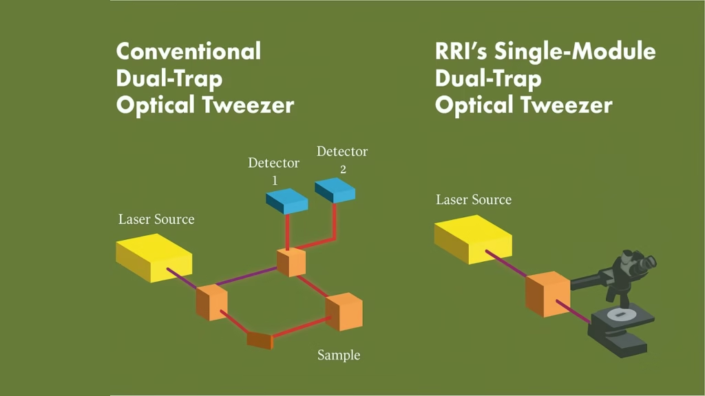
The new system pioneers a confocal detection scheme. In a media statement, Md Arsalan Ashraf, a doctoral scholar at RRI, explained, “The unique optical trapping scheme utilizes laser light scattered back by the sample for detecting trapped particle position. This technique pushes past some of the long-standing constraints of dual-trap configurations and removes signal interference. The single-module design integrates effortlessly with standard microscopy frameworks,” he said.
The refinement doesn’t end there. The system ensures that detectors tracking tiny particles remain perfectly aligned, even when the optical traps themselves move. The result: two stable, reliable measurement channels, zero interference, and no need for complicated re-adjustment mid-experiment—a frequent headache with older systems.
Traditional dual-trap designs have required costly and complex add-ons, sometimes even hijacking the features of laboratory microscopes and making additional techniques, such as phase contrast or fluorescence imaging, hard to use. “This new single-module trapping and detection design makes high-precision force measurement studies of single molecules, probing of soft materials including biological samples, and micromanipulation of biological samples like cells much more convenient and cost-effective,” said Pramod A Pullarkat, lead principal investigator at RRI, in a statement.
By removing cross-talk and offering robust stability—whether traps are close together, displaced, or the environment changes—the RRI team’s approach is not only easier to use but far more adaptable. Its plug-and-play module fits onto standard microscopes without overhauling their basic structure.
From the intellectual property point of view, this design may be a game-changer. By cracking the persistent problem of signal interference with minimalist engineering, the new setup enhances measurement precision and reliability—essential advantages for researchers performing delicate biophysical experiments on everything from molecular motors to living cells.
With the essential building blocks in place, the RRI team is now exploring commercial avenues to produce and distribute their single-module, dual-trap optical tweezer system as an affordable add-on for existing microscopes. The innovation stands to put advanced single-molecule force spectroscopy, long limited to wealthier labs abroad, into the hands of scientists across India—and perhaps spark breakthroughs across the biomedical sciences.
Space & Physics
New Magnetic Transistor Breakthrough May Revolutionize Electronics
A team of MIT physicists has created a magnetic transistor that could make future electronics smaller, faster, and more energy-efficient. By swapping silicon for a new magnetic semiconductor, they’ve opened the door to game-changing advancements in computing.

For decades, silicon has been the undisputed workhorse in transistors—the microscopic switches responsible for processing information in every phone, computer, and high-tech device. But silicon’s physical limits have long frustrated scientists seeking ever-smaller, more efficient electronics.
Now, MIT researchers have unveiled a major advance: they’ve replaced silicon with a magnetic semiconductor, introducing magnetism into transistors in a way that promises tighter, smarter, and more energy-saving circuits. This new ingredient, chromium sulfur bromide, makes it possible to control electricity flow with far greater efficiency and could even allow each transistor to “remember” information, simplifying circuit design for future chips.
“This lack of contamination enables their device to outperform existing magnetic transistors. Most others can only create a weak magnetic effect, changing the flow of current by a few percent or less. Their new transistor can switch or amplify the electric current by a factor of 10,” the MIT team said in a media statement. Their work, detailed in Physical Review Letters, outlines how this material’s stability and clean switching between magnetic states unlocks a new degree of control.
Chung-Tao Chou, MIT graduate student and co-lead author, explains in a media statement, “People have known about magnets for thousands of years, but there are very limited ways to incorporate magnetism into electronics. We have shown a new way to efficiently utilize magnetism that opens up a lot of possibilities for future applications and research.”
The device’s game-changing aspect is its ability to combine the roles of memory cell and transistor, allowing electronics to read and store information faster and more reliably. “Now, not only are transistors turning on and off, they are also remembering information. And because we can switch the transistor with greater magnitude, the signal is much stronger so we can read out the information faster, and in a much more reliable way,” said Luqiao Liu, MIT associate professor, in a media statement.
Moving forward, the team is looking to scale up their clean manufacturing process, hoping to create arrays of these magnetic transistors for broader commercial and scientific use. If successful, the innovation could usher in a new era of spintronic devices, where magnetism becomes as central to electronics as silicon is today.


The Data Don’t Lie: Women Are Still Missing from Science — But Why?

Global Report Reveals Planetary Health Communication Crisis Fuelled by AI and Misinformation

MIT Engineers’ Discovery Could Supercharge Hydrogen Economy

Bridging the Adaptation Finance Gap: India’s Case Before COP30

The Dragon and the Elephant Dance for a Cleaner World

The Next Green Revolution Is Being Built on China’s Terms

Most Earthquake Energy Is Spent Heating Up Rocks, Not Shaking the Ground: New MIT Study Finds

Why Kerala Has Struggled to Replicate Perinjanam’s Solar Success

Study Suggests Primordial Black Hole Explosions May Explain Highest-Energy Neutrino Detected

The Tiny Grip That Could Reshape Medicine: India’s Dual-Trap Optical Tweezer

-

 Space & Physics5 months ago
Is Time Travel Possible? Exploring the Science Behind the Concept
-

 Earth6 months ago
122 Forests, 3.2 Million Trees: How One Man Built the World’s Largest Miyawaki Forest
-

 Space & Physics6 months ago
Did JWST detect “signs of life” in an alien planet?
-

 Know The Scientist5 months ago
Narlikar – the rare Indian scientist who penned short stories
-

 Society4 months ago
Shukla is now India’s first astronaut in decades to visit outer space
-

 Society4 months ago
Axiom-4 will see an Indian astronaut depart for outer space after 41 years
-

 Earth4 months ago
World Environment Day 2025: “Beating plastic pollution”
-

 Society6 months ago
Rabies, Bites, and Policy Gaps: One Woman’s Humane Fight for Kerala’s Stray Dogs