Space & Physics
India’s quantum leap: The future of computing and research
Quantum computers, with their ability to process complex calculations at speeds unattainable by classical computers, are expected to unlock new realms of possibility in artificial intelligence, cryptography, and material sciences

On September 26, Indian Prime Minister Narendra Modi dedicated three indigenously developed PARAM (Parallel Machine) Rudra Supercomputers to the nation, marking a significant stride in India’s scientific capabilities. Priced at approximately Rs 130 crore, these supercomputers are now operational in India’s major cities-Pune, Delhi, and Kolkata, enhancing the nation’s research capabilities across diverse fields including physics, earth sciences, and cosmology.
While the new move is a testament to India’s growing technological prowess, it is the country’s ambition in quantum computing that promises to revolutionize the landscape of scientific research. The Prime Minister underscored this ambition during his address, emphasizing that the future of technology lies in harnessing quantum computing’s unparalleled potential.
The National Quantum Mission, launched to propel India to the forefront of this cutting-edge field, reflects a grand vision of transforming traditional computing paradigms. Quantum computers, with their ability to process complex calculations at speeds unattainable by classical computers, are expected to unlock new realms of possibility in artificial intelligence, cryptography, and material sciences. As the Prime Minister stated, “This emerging technology is expected to transform the world, bringing unprecedented changes to the IT sector, manufacturing, small enterprises, and startups.”
This focus on quantum technology aligns seamlessly with the establishment of the PARAM Rudra Supercomputers. These machines will serve not only as a backbone for advanced scientific research but also as critical infrastructure for developing quantum algorithms and applications. The interdependence of supercomputers and quantum computing signifies a dual pathway for India’s technological advancement, where both realms can enhance one another.
As India aspires to lead globally in these high-tech domains, the implications extend beyond academic circles. The integration of supercomputers with quantum computing capabilities is poised to catalyse innovative solutions that can address pressing societal challenges, from climate change predictions to optimizing agricultural practices. The recently inaugurated High-Performance Computing system, tailored for weather and climate research, exemplifies this potential. With its advanced predictive models, it is set to empower farmers and fishermen, ensuring they have access to critical data that can enhance their livelihoods.
India’s focus on youth and education—through initiatives like the establishment of Atal Tinkering Labs and increased scholarships for STEM education—demonstrates a concerted effort to nurture the next generation of scientists and engineers who will drive the nation’s ambitions in both supercomputing and quantum technology.
As India continues to make remarkable strides in various sectors, including space and semiconductor technologies, the integration of supercomputing and quantum capabilities is poised to redefine the country’s position on the global stage. The Prime Minister’s optimism about India’s future in these domains reflects a broader narrative of a nation ready to leverage its scientific advancements for both national development and global leadership.
While the PARAM Rudra Supercomputers represent a monumental step forward, it is the path toward quantum computing that holds the promise of transformative change. With the right investments and a robust scientific community, India is not just aiming to keep pace with global advancements but is setting the stage to lead in the realms of technology that will shape the future.
Space & Physics
Atoms Speak Out: Physicists Use Electrons as Messengers to Unlock Secrets of the Nucleus
Physicists at MIT have devised a table-top method to peer inside an atom’s nucleus using the atom’s own electrons

Physicists at MIT have developed a pioneering method to look inside an atom’s nucleus — using the atom’s own electrons as tiny messengers within molecules rather than massive particle accelerators.
In a study published in Science, the researchers demonstrated this approach using molecules of radium monofluoride, which pair a radioactive radium atom with a fluoride atom. The molecules act like miniature laboratories where electrons naturally experience extremely strong electric fields. Under these conditions, some electrons briefly penetrate the radium nucleus, interacting directly with protons and neutrons inside. This rare intrusion leaves behind a measurable energy shift, allowing scientists to infer details about the nucleus’ internal structure.
The team observed that these energy shifts, though minute — about one millionth of the energy of a laser photon — provide unambiguous evidence of interactions occurring inside the nucleus rather than outside it. “We now have proof that we can sample inside the nucleus,” said Ronald Fernando Garcia Ruiz, the Thomas A. Franck Associate Professor of Physics at MIT, in a statement. “It’s like being able to measure a battery’s electric field. People can measure its field outside, but to measure inside the battery is far more challenging. And that’s what we can do now.”
Traditionally, exploring nuclear interiors required kilometer-long particle accelerators to smash high-speed beams of electrons into targets. The MIT technique, by contrast, achieves similar insight with a table-top molecular setup. It makes use of the molecule’s natural electric environment to magnify these subtle interactions.
The radium nucleus, unlike most which are spherical, has an asymmetric “pear” shape that makes it a powerful system for studying violations of fundamental physical symmetries — phenomena that could help explain why the universe contains far more matter than antimatter. “The radium nucleus is predicted to be an amplifier of this symmetry breaking, because its nucleus is asymmetric in charge and mass, which is quite unusual,” Garcia Ruiz explained.
To conduct their experiments, the researchers produced radium monofluoride molecules at CERN’s Collinear Resonance Ionization Spectroscopy (CRIS) facility, trapped and cooled them in laser-guided chambers, and then measured laser-induced energy transitions with extreme precision. The work involved MIT physicists Shane Wilkins, Silviu-Marian Udrescu, and Alex Brinson, alongside international collaborators.
“Radium is naturally radioactive, with a short lifetime, and we can currently only produce radium monofluoride molecules in tiny quantities,” said Wilkins. “We therefore need incredibly sensitive techniques to be able to measure them.”
As Udrescu added, “When you put this radioactive atom inside of a molecule, the internal electric field that its electrons experience is orders of magnitude larger compared to the fields we can produce and apply in a lab. In a way, the molecule acts like a giant particle collider and gives us a better chance to probe the radium’s nucleus.”
Going forward, the MIT team aims to cool and align these molecules so that the orientation of their pear-shaped nuclei can be controlled for even more detailed mapping. “Radium-containing molecules are predicted to be exceptionally sensitive systems in which to search for violations of the fundamental symmetries of nature,” Garcia Ruiz said. “We now have a way to carry out that search”
Space & Physics
Physicists Double Precision of Optical Atomic Clocks with New Laser Technique
MIT researchers develop a quantum-enhanced method that doubles the precision and stability of optical atomic clocks, paving the way for portable, ultra-accurate timekeeping.
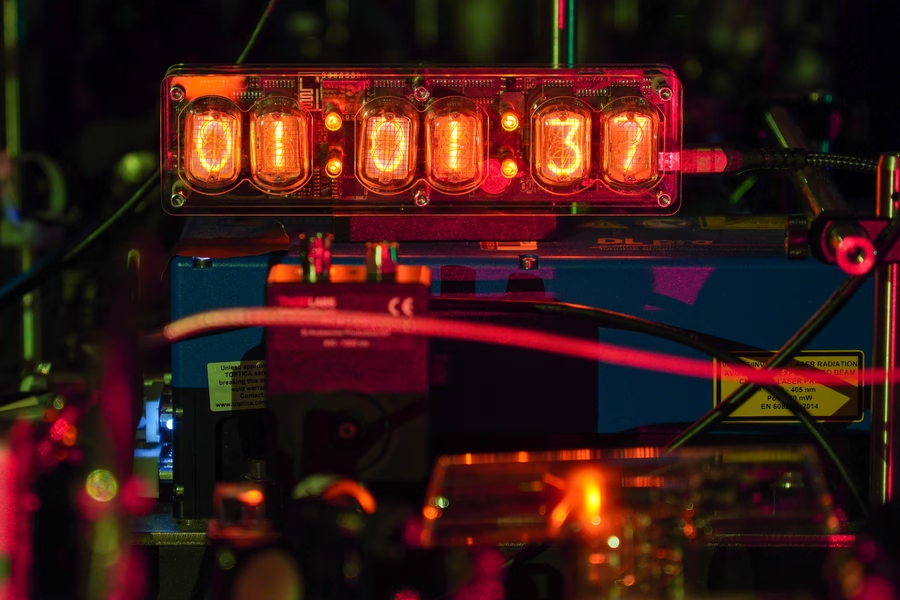
MIT physicists have unveiled a new technique that could significantly improve the precision and stability of next-generation optical atomic clocks, devices that underpin everything from mobile transactions to navigation apps. In a recent media statement, the MIT team explained: “Every time you check the time on your phone, make an online transaction, or use a navigation app, you are depending on the precision of atomic clocks. An atomic clock keeps time by relying on the ‘ticks’ of atoms as they naturally oscillate at rock-steady frequencies.”
Current atomic clocks rely on cesium atoms tracked with lasers at microwave frequencies, but scientists are advancing to clocks based on faster-ticking atoms like ytterbium, which can be tracked with lasers at higher, optical frequencies and discern intervals up to 100 trillion times per second.
A research group at MIT, led by Vladan Vuletić, the Lester Wolfe Professor of Physics, detailed that their newly developed method harnesses a laser-induced “global phase” in ytterbium atoms and boosts this effect using quantum amplification. Vuletić stated, “We think our method can help make these clocks transportable and deployable to where they’re needed.” The approach, called global phase spectroscopy, doubles the precision of an optical atomic clock, enabling it to resolve twice as many ticks per second compared to standard setups, and promises further gains with increasing atom counts.
The technique could pave the way for portable optical atomic clocks able to measure all manner of phenomena in various locations. Vuletić summarized the broader scientific ambitions: “With these clocks, people are trying to detect dark matter and dark energy, and test whether there really are just four fundamental forces, and even to see if these clocks can predict earthquakes.”
The MIT team has previously demonstrated improved clock precision by quantumly entangling hundreds of ytterbium atoms and using time reversal tricks to amplify their signals. Their latest advance applies these methods to much faster optical frequencies, where stabilizing the clock laser has always been a major challenge. “When you have atoms that tick 100 trillion times per second, that’s 10,000 times faster than the frequency of microwaves,” said Vuletić in the statement. Their experiments revealed a surprisingly useful “global phase” information about the laser frequency, previously thought irrelevant, unlocking the potential for even greater accuracy.
The research, led by Vuletić and joined by Leon Zaporski, Qi Liu, Gustavo Velez, Matthew Radzihovsky, Zeyang Li, Simone Colombo, and Edwin Pedrozo-Peñafiel of the MIT-Harvard Center for Ultracold Atoms, was published in Nature. They believe the technical benefits of the new method will make atomic clocks easier to run and enable stable, transportable clocks fit for future scientific exploration, including earthquake prediction, fundamental physics, and global time standards.
Space & Physics
Nobel Prize in Physics: Clarke, Devoret, and Martinis Honoured for Pioneering Quantum Discoveries
The 2025 Nobel Prize in Physics honours John Clarke, Michel H. Devoret, and John M. Martinis for revealing how entire electrical circuits can display quantum behaviour — a discovery that paved the way for modern quantum computing.
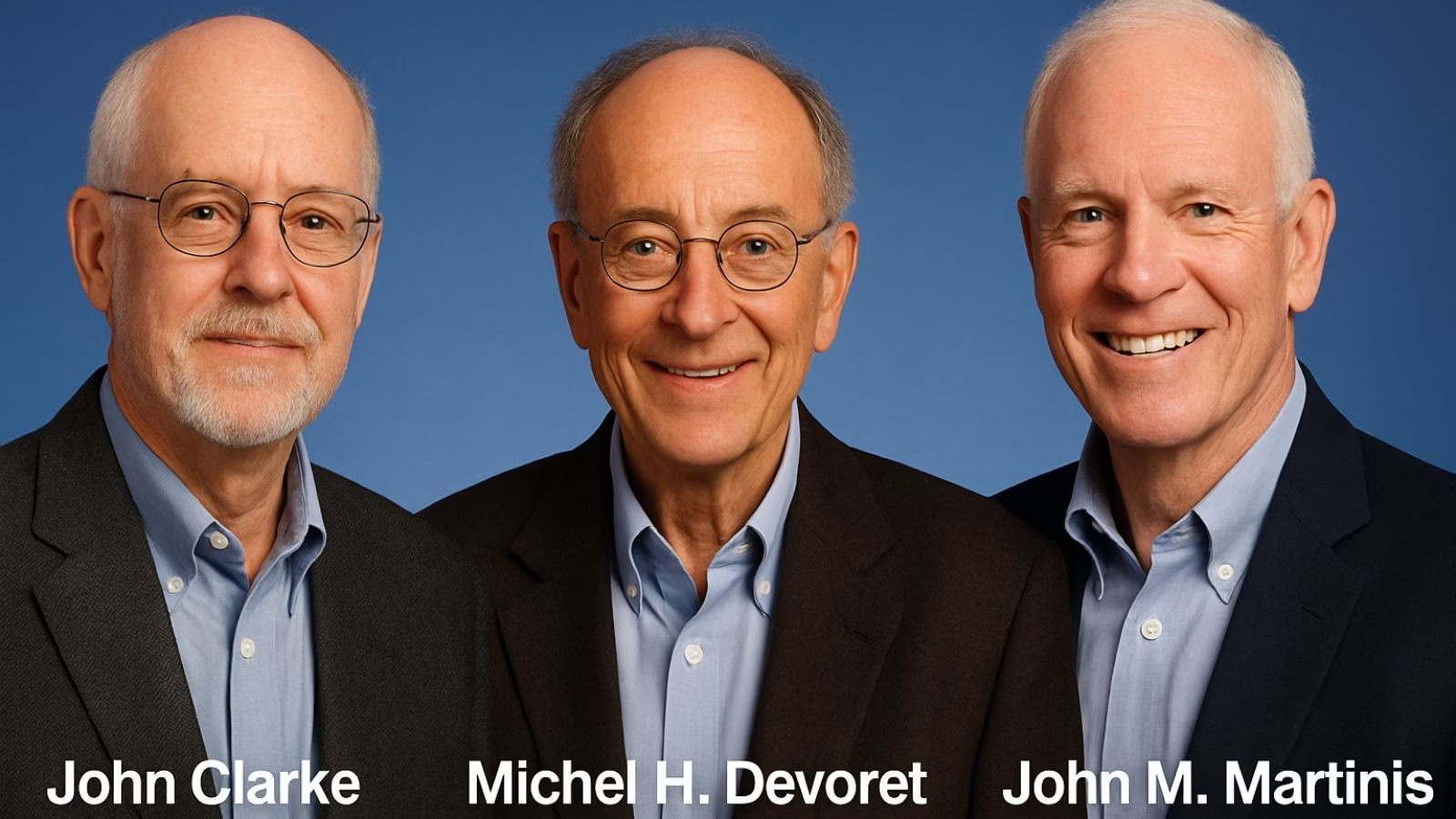
The 2025 Nobel Prize in Physics has been awarded to John Clarke, Michel H. Devoret, and John M. Martinis for their landmark discovery of macroscopic quantum mechanical tunnelling and energy quantisation in an electric circuit, an innovation that laid the foundation for today’s quantum computing revolution.
Announcing the prize, Olle Eriksson, Chair of the Nobel Committee for Physics, said, “It is wonderful to be able to celebrate the way that century-old quantum mechanics continually offers new surprises. It is also enormously useful, as quantum mechanics is the foundation of all digital technology.”
The Committee described their discovery as a “turning point in understanding how quantum mechanics manifests at the macroscopic scale,” bridging the gap between classical electronics and quantum physics.
John Clarke: The SQUID Pioneer
British-born John Clarke, Professor Emeritus at the University of California, Berkeley, is celebrated for his pioneering work on Superconducting Quantum Interference Devices (SQUIDs) — ultra-sensitive detectors of magnetic flux. His career has been marked by contributions that span superconductivity, quantum amplifiers, and precision measurements.
Clarke’s experiments in the early 1980s provided the first clear evidence of quantum behaviour in electrical circuits — showing that entire electrical systems, not just atoms or photons, can obey the strange laws of quantum mechanics.
A Fellow of the Royal Society, Clarke has been honoured with numerous awards including the Comstock Prize (1999) and the Hughes Medal (2004).
Michel H. Devoret: Architect of Quantum Circuits
French physicist Michel H. Devoret, now the Frederick W. Beinecke Professor Emeritus of Applied Physics at Yale University, has been one of the intellectual architects of quantronics — the study of quantum phenomena in electrical circuits.
After earning his PhD at the University of Paris-Sud and completing a postdoctoral fellowship under Clarke at Berkeley, Devoret helped establish the field of circuit quantum electrodynamics (cQED), which underpins the design of modern superconducting qubits.
His group’s innovations — from the single-electron pump to the fluxonium qubit — have set performance benchmarks in quantum coherence and control. Devoret is also a recipient of the Fritz London Memorial Prize (2014) and the John Stewart Bell Prize, and is a member of the French Academy of Sciences.
John M. Martinis: Building the Quantum Processor
American physicist John M. Martinis, who completed his PhD at UC Berkeley under Clarke’s supervision, translated these quantum principles into the hardware era. His experiments demonstrated energy level quantisation in Josephson junctions, one of the key results now honoured by the Nobel Committee.
Martinis later led Google’s Quantum AI lab, where his team in 2019 achieved the world’s first demonstration of quantum supremacy — showing a superconducting processor outperforming the fastest classical supercomputer on a specific task.
A former professor at UC Santa Barbara, Martinis continues to be a leading voice in quantum computing research and technology development.
A Legacy of Quantum Insight
Together, the trio’s discovery, once seen as a niche curiosity in superconducting circuits, has become the cornerstone of the global quantum revolution. Their experiments proved that macroscopic electrical systems can display quantised energy states and tunnel between them, much like subatomic particles.
Their work, as the Nobel citation puts it, “opened a new window into the quantum behaviour of engineered systems, enabling technologies that are redefining computation, communication, and sensing.”


Atoms Speak Out: Physicists Use Electrons as Messengers to Unlock Secrets of the Nucleus

Guterres to WMO: ‘No Country Is Safe Without Early Warnings’

Farmers Warn: The World Needs $443 Billion a Year to Protect Those Feeding Half of Humanity

When the Floods Cleared the Skies, and Firecrackers Choked Them Again

Global Warming Supercharges India’s Monsoon, Drives Rainfall Extremes: New Analysis finds

Why Kerala Has Struggled to Replicate Perinjanam’s Solar Success

The Tiny Grip That Could Reshape Medicine: India’s Dual-Trap Optical Tweezer

Bridging the Adaptation Finance Gap: India’s Case Before COP30

Madhya Pradesh: Crop Damage Due to Excessive Rain—What Could Be the Solution?

Earth Nears Dangerous Tipping Points Amid Rapid Warming, Urgent Action Needed at COP30

 Space & Physics5 months ago
Is Time Travel Possible? Exploring the Science Behind the Concept
- Know The Scientist5 months ago
Narlikar – the rare Indian scientist who penned short stories
- Society4 months ago
Shukla is now India’s first astronaut in decades to visit outer space
- Earth5 months ago
World Environment Day 2025: “Beating plastic pollution”
- Society5 months ago
Axiom-4 will see an Indian astronaut depart for outer space after 41 years
- The Sciences4 months ago
How a Human-Inspired Algorithm Is Revolutionizing Machine Repair Models in the Wake of Global Disruptions
- Space & Physics3 months ago
Joint NASA-ISRO radar satellite is the most powerful built to date
- Space & Physics6 months ago
MIT Physicists Capture First-Ever Images of Freely Interacting Atoms in Space