Space & Physics
JWST unveils a neutron star in supernova remnant
The neutron star detection was made possible with the James Webb Space Telescope (JWST) infrared detectors.
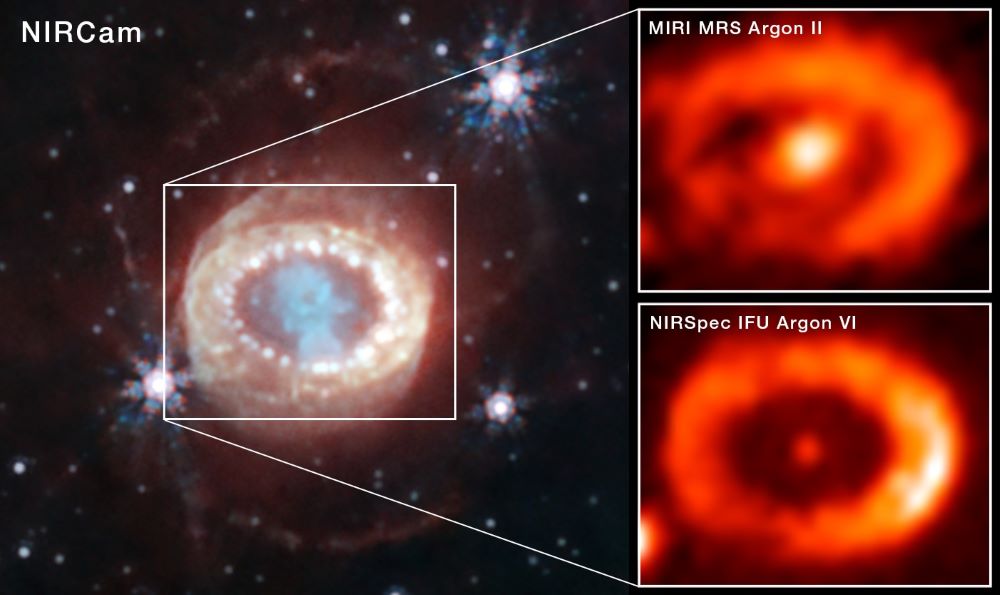
A team of astrophysicists used the James Webb Space Telescope (JWST) to confirm presence of a neutron star within the explosive remnants of the SN 1987A supernova.
The eponymous SN 1987A remains the only supernova in the past few centuries to have been visible in the sky – even in daytime.
Previous research into the supernova remnant didn’t yield conclusive evidence in favor of a neutron star. They ruled out black holes too. The new research makes it as conclusive as it can get.
Also, it’s the first time that tell-tale signs of a neutron star signature were detected from any supernova event. “We have not observed any compelling signature of such a newborn object from any supernova explosion,” said first author Claes Fransson, an astrophysicist at Stockholm University to NASA. “With this observatory, we have now found direct evidence for emission triggered by the newborn compact object, most likely a neutron star.”
The JWST’s MIRI (or Mid-Infrared Instrument) and NIRcam (or Near Infrared Camera) detected the radiation in infrared.
A supernova event marks the end of the first phase of a massive star’s life, when a star runs out of fuel required to maintain nuclear fusion. In this case, the star’s core collapsed inward, producing a neutron star while the outer layers of the host star were shed away in a cataclysmic explosion.
In SN1987a’s case, the host star was a blue supergiant. Our sun in comparison is a low mass star, and evolves differently when it ages.
The paper suggests the neutron star born from SN 1987A may have reached as much as at least 100 billion degrees Celsius in the immediate aftermath of the 1987 supernova event.
Now 37 years later, the star cooled to at most 3 million degrees Celsius. Our sun is pale in comparison, at 5,600 degree Celsius.
Argon gas not so ‘noble’ anymore
The neutron star’s intense radiation managed to heat even argon gas from the remnant, which forced the gas in turn to emit its own radiation. It’s this radiation in the infrared wavelength that was detected by JWST. Other wavelengths detected include sulfur gas, silicates and graphite that form dust.
This is surprising since argon exists on earth as a chemically un-reactive gas, in standard temperature and pressure conditions. Although astrophysicists have known for over a decade that supernova events can ‘ionize’ argon gas, it’s just not so often that these type of events occur.
The researchers believe the argon was formed by the nuclear fusion of oxygen and silicon from the parent blue supergiant.
“To create these ions that we observed in the ejecta, it was clear that there had to be a source of high-energy radiation in the center of the SN 1987A remnant,” said Fransson. “In the paper we discuss different possibilities, finding that only a few scenarios are likely, and all of these involve a newly born neutron star.”
However, the researchers aren’t sure what sub-type of neutron star they could have detected. It’s either a ‘cooling neutron star’ or a ‘pulsar wind nebulae’ that’s the source of the radiation.
The researchers claimed to have done their analysis systematically, ruling out any alternatives in place of the supposed neutron star.
The research, published in Science, was funded by the space agencies of Sweden, Europe, the UK and the US. Others included the Knut and Alice Wallenberg Foundation, European Research Council, Science Foundation Ireland/Irish Research Council Pathway program, UK Science and Technology Facilities Council (STFC), STFC Webb fellowship, California Institute of Technology, Spanish Ministry of Science and Innovation/State Agency of Research, Belgian Science Policy Office (BELSPO) for the provision of financial support in the framework of the PRODEX program of the European Space Agency (ESA).


Space & Physics
MIT Pioneers Real-Time Observation of Unconventional Superconductivity in Magic-Angle Graphene
Physicists have directly observed unconventional superconductivity in magic-angle twisted tri-layer graphene using a new experimental platform, revealing a unique pairing mechanism
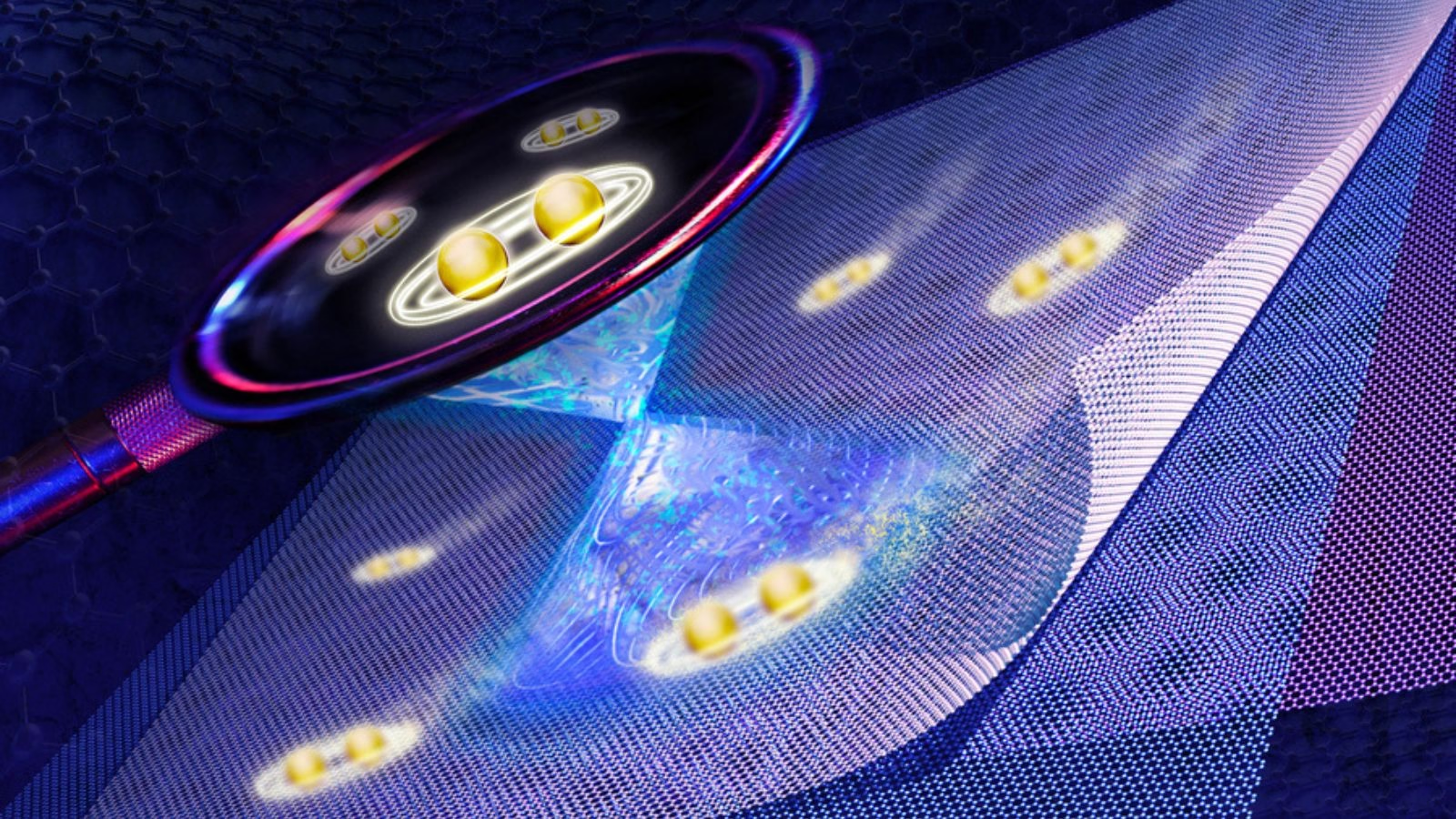
MIT physicists have unveiled compelling direct evidence for unconventional superconductivity in “magic-angle” twisted tri-layer graphene—an atomically engineered material that could reimagine the future of energy transport and quantum technologies. Their new experiment marks a pivotal step forward, offering a fresh perspective on how electrons synchronize in precisely stacked two-dimensional materials, potentially laying the groundwork for next-generation superconductors that function well above current temperature limits.
Instead of looking merely at theoretical possibilities, the MIT team built a novel platform that lets researchers visualize the superconducting gap “as it emerges in real-time within 2D materials,” said co-lead author Shuwen Sun in a media statement. This gap is crucial, reflecting how robust the material’s superconducting state is during temperature changes—a key indicator for practical applications.
What’s striking, said Jeong Min Park, study co-lead author, is that the superconducting gap in magic-angle graphene differs starkly from the smooth, uniform profile seen in conventional superconductors. “We observed a V-shaped gap that reveals an entirely new pairing mechanism—possibly driven by the electrons themselves, rather than crystal vibrations,” Park said. Such direct measurement is a “first” for the field, giving scientists a more refined tool for identifying and understanding unconventional superconductivity.
Senior author Pablo Jarillo-Herrero emphasized that their method could help crack the code behind room-temperature superconductors: “This breakthrough may trigger deeper insights not just for graphene, but for the entire class of twistronic materials. Imagine grids and quantum computers that operate with zero energy loss—this is the holy grail we’re moving toward,” Jarillo-Herrero said in the MIT release.
Collaborators included scientists from Japan’s National Institute for Materials Science, broadening the impact of the research. The discovery builds on years of progress since the first magic-angle graphene experiments in 2018, opening what many now call the “twistronics” era—a field driven by stacking and twisting atom-thin materials to unlock uniquely quantum properties.
Looking ahead, the team plans to expand its analysis to other ultra-thin structures, hoping to map out electronic behavior not only for superconductors, but for a wider range of correlated quantum phases. “We can now directly observe electron pairs compete and coexist with other quantum states—this could allow us to design new materials from the ground up,” said Park in her public statement.
The research underscores the value of visualization in fundamental physics, suggesting that direct observation may be the missing link to controlling quantum phenomena for efficient, room-temperature technology.
Space & Physics
Atoms Speak Out: Physicists Use Electrons as Messengers to Unlock Secrets of the Nucleus
Physicists at MIT have devised a table-top method to peer inside an atom’s nucleus using the atom’s own electrons

Physicists at MIT have developed a pioneering method to look inside an atom’s nucleus — using the atom’s own electrons as tiny messengers within molecules rather than massive particle accelerators.
In a study published in science, the researchers demonstrated this approach using molecules of radium monofluoride, which pair a radioactive radium atom with a fluoride atom. The molecules act like miniature laboratories where electrons naturally experience extremely strong electric fields. Under these conditions, some electrons briefly penetrate the radium nucleus, interacting directly with protons and neutrons inside. This rare intrusion leaves behind a measurable energy shift, allowing scientists to infer details about the nucleus’ internal structure.
The team observed that these energy shifts, though minute — about one millionth of the energy of a laser photon — provide unambiguous evidence of interactions occurring inside the nucleus rather than outside it. “We now have proof that we can sample inside the nucleus,” said Ronald Fernando Garcia Ruiz, the Thomas A. Franck Associate Professor of Physics at MIT, in a statement. “It’s like being able to measure a battery’s electric field. People can measure its field outside, but to measure inside the battery is far more challenging. And that’s what we can do now.”
Traditionally, exploring nuclear interiors required kilometer-long particle accelerators to smash high-speed beams of electrons into targets. The MIT technique, by contrast, achieves similar insight with a table-top molecular setup. It makes use of the molecule’s natural electric environment to magnify these subtle interactions.
The radium nucleus, unlike most which are spherical, has an asymmetric “pear” shape that makes it a powerful system for studying violations of fundamental physical symmetries — phenomena that could help explain why the universe contains far more matter than antimatter. “The radium nucleus is predicted to be an amplifier of this symmetry breaking, because its nucleus is asymmetric in charge and mass, which is quite unusual,” Garcia Ruiz explained.
To conduct their experiments, the researchers produced radium monofluoride molecules at CERN’s Collinear Resonance Ionization Spectroscopy (CRIS) facility, trapped and cooled them in laser-guided chambers, and then measured laser-induced energy transitions with extreme precision. The work involved MIT physicists Shane Wilkins, Silviu-Marian Udrescu, and Alex Brinson, alongside international collaborators.
“Radium is naturally radioactive, with a short lifetime, and we can currently only produce radium monofluoride molecules in tiny quantities,” said Wilkins. “We therefore need incredibly sensitive techniques to be able to measure them.”
As Udrescu added, “When you put this radioactive atom inside of a molecule, the internal electric field that its electrons experience is orders of magnitude larger compared to the fields we can produce and apply in a lab. In a way, the molecule acts like a giant particle collider and gives us a better chance to probe the radium’s nucleus.”
Going forward, the MIT team aims to cool and align these molecules so that the orientation of their pear-shaped nuclei can be controlled for even more detailed mapping. “Radium-containing molecules are predicted to be exceptionally sensitive systems in which to search for violations of the fundamental symmetries of nature,” Garcia Ruiz said. “We now have a way to carry out that search”
Space & Physics
Physicists Double Precision of Optical Atomic Clocks with New Laser Technique
MIT researchers develop a quantum-enhanced method that doubles the precision and stability of optical atomic clocks, paving the way for portable, ultra-accurate timekeeping.
MIT physicists have unveiled a new technique that could significantly improve the precision and stability of next-generation optical atomic clocks, devices that underpin everything from mobile transactions to navigation apps. In a recent media statement, the MIT team explained: “Every time you check the time on your phone, make an online transaction, or use a navigation app, you are depending on the precision of atomic clocks. An atomic clock keeps time by relying on the ‘ticks’ of atoms as they naturally oscillate at rock-steady frequencies.”
Current atomic clocks rely on cesium atoms tracked with lasers at microwave frequencies, but scientists are advancing to clocks based on faster-ticking atoms like ytterbium, which can be tracked with lasers at higher, optical frequencies and discern intervals up to 100 trillion times per second.
A research group at MIT, led by Vladan Vuletić, the Lester Wolfe Professor of Physics, detailed that their newly developed method harnesses a laser-induced “global phase” in ytterbium atoms and boosts this effect using quantum amplification. Vuletić stated, “We think our method can help make these clocks transportable and deployable to where they’re needed.” The approach, called global phase spectroscopy, doubles the precision of an optical atomic clock, enabling it to resolve twice as many ticks per second compared to standard setups, and promises further gains with increasing atom counts.
The technique could pave the way for portable optical atomic clocks able to measure all manner of phenomena in various locations. Vuletić summarized the broader scientific ambitions: “With these clocks, people are trying to detect dark matter and dark energy, and test whether there really are just four fundamental forces, and even to see if these clocks can predict earthquakes.”
The MIT team has previously demonstrated improved clock precision by quantumly entangling hundreds of ytterbium atoms and using time reversal tricks to amplify their signals. Their latest advance applies these methods to much faster optical frequencies, where stabilizing the clock laser has always been a major challenge. “When you have atoms that tick 100 trillion times per second, that’s 10,000 times faster than the frequency of microwaves,” said Vuletić in the statement. Their experiments revealed a surprisingly useful “global phase” information about the laser frequency, previously thought irrelevant, unlocking the potential for even greater accuracy.
The research, led by Vuletić and joined by Leon Zaporski, Qi Liu, Gustavo Velez, Matthew Radzihovsky, Zeyang Li, Simone Colombo, and Edwin Pedrozo-Peñafiel of the MIT-Harvard Center for Ultracold Atoms, was published in Nature. They believe the technical benefits of the new method will make atomic clocks easier to run and enable stable, transportable clocks fit for future scientific exploration, including earthquake prediction, fundamental physics, and global time standards.


India Among World’s 10 Most Affected Nations from Extreme Weather

Over 832,000 Lives Lost, $4.5 Trillion in Damages, Extreme Weather The “New Normal”: Warns Climate Risk Index

COP30: How People, Not Politics, Are Powering the Next Phase of Climate Action

MIT Pioneers Real-Time Observation of Unconventional Superconductivity in Magic-Angle Graphene

Brazil Cuts Emissions by 17% in 2024—Biggest Drop in 16 Years, Yet Paris Target Out of Reach

Atoms Speak Out: Physicists Use Electrons as Messengers to Unlock Secrets of the Nucleus

Earth Nears Dangerous Tipping Points Amid Rapid Warming, Urgent Action Needed at COP30

India and China to Peak Coal Emissions by 2030 — and India’s Data Proves It’s Economically Inevitable

Farmers Warn: The World Needs $443 Billion a Year to Protect Those Feeding Half of Humanity

Guterres to WMO: ‘No Country Is Safe Without Early Warnings’
-

 Space & Physics6 months ago
Is Time Travel Possible? Exploring the Science Behind the Concept
-

 Know The Scientist6 months ago
Narlikar – the rare Indian scientist who penned short stories
-

 Know The Scientist5 months ago
Remembering S.N. Bose, the underrated maestro in quantum physics
-
 Space & Physics3 months ago
Joint NASA-ISRO radar satellite is the most powerful built to date
-

 Society5 months ago
Axiom-4 will see an Indian astronaut depart for outer space after 41 years
-

 Society5 months ago
Shukla is now India’s first astronaut in decades to visit outer space
-

 Society5 months ago
Why the Arts Matter As Much As Science or Math
-

 Earth5 months ago
World Environment Day 2025: “Beating plastic pollution”