Space & Physics
Why does superconductivity matter?
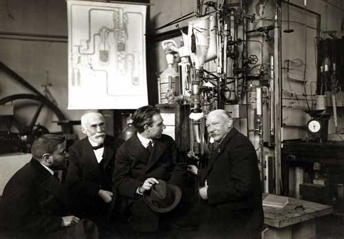
Superconductivity was discovered by H. Kamerlingh Onnes on April 8, 1911, who was studying the resistance of solid Mercury (Hg) at cryogenic temperatures. Liquid helium was recently discovered at that time. At T = 4.2K, the resistance of Hg disappeared abruptly. This marked a transition to a new phase that was never seen before. The state is resistanceless, strongly diamagnetic, and denotes a new state of matter. K. Onnes sent two reports to KNAW (the local journal of the Netherlands), where he preferred calling the zero-resistance state ‘superconductivity’’.
There was another discovery that went unnoticed in the same experiment, which was the transition of superfluid Helium (He) at 2.2K, the so-called λ transition, below which He becomes a superfluid. However, we shall skip that discussion for now. A couple of years later, superconductivity was found in lead (Pb) at 7K. Much later, in 1941, Niobium Nitride was found to superconduct below 16 K. The burning question in those days was: what would the conductivity or resistivity of metals be at a very low temperature?
The reason behind such a question is Lord Kelvin’s suggestion that for metals, initially the resistivity decreases with falling temperature and finally climbs to infinity at zero Kelvin because electrons’ mobility becomes zero at 0 K, yielding zero conductivity and hence infinite resistivity. Kamerlingh Onnes and his assistant Jacob Clay studied the resistance of gold (Au) and platinum (Pt) down to T = 14K. There was a linear decrease in resistance until 14 K; however, lower temperatures cannot be accessed owing to the unavailability of liquid He, which eventually happened in 1908.
In fact, the experiment with Au and Pt was repeated after 1908. For Pt, the resistivity became constant after 4.2K, while Au is found to superconduct at very low temperatures. Thus, Lord Kelvin’s notion about infinite resistivity at very low temperatures was incorrect. Onnes had found that at 3 K (below the transition), the normalised resistance is about 10−7. Above 4.2 K, the resistivity starts appearing again. The transition is too sharp and falls abruptly to zero within a temperature window of 10−4 K.
All superconductors are normal metals above the transition temperature. If we ask in the periodic table where most of the superconductors are located, the answer throws some surprises. The good metals are rarely superconducting
Perfect conductors, superconductors, and magnets
All superconductors are normal metals above the transition temperature. If we ask in the periodic table where most of the superconductors are located, the answer throws some surprises. The good metals are rarely superconducting. The examples are Ag, Au, Cu, Cs, etc., which have transition temperatures of the order of ∼ 0.1K, while the bad metals, such as niobium alloys, copper oxides, and 1 MgB2, have relatively larger transition temperatures. Thus, bad metals are, in general, good superconductors. An important quantity in this regard is the mean free path of the electrons. The mean free path is of the order of a few A0 for metals (above Tc), while for good metals (or the bad superconductors), it is usually a few hundred of A0. Whereas for the bad metals (good superconductors), it is still small as the electrons are strongly coupled to phonons. The orbital overlap is large in a superconductor. In good metals, the orbital overlap is small, and often they become good magnets. In the periodic table, transition elements such as the 3D series elements, namely Al, Bi, Cd, Ga, etc., become good superconductors, while Cr, Mn, and Fe are bad superconductors and in fact form good magnets. For all of them, that is, whether they are superconductors or magnets, there is a large density of states at the Fermi level. So, a lot of electronic states are necessary for the electrons in these systems to be able to condense into a superconducting state (or even a magnetic state). The nature of the electronic wave function determines whether they develop superconducting order or magnetic order. For example, electronic wavefunctions have a large spatial extent for superconductors, while they are short-range for magnets.
Meissner effect
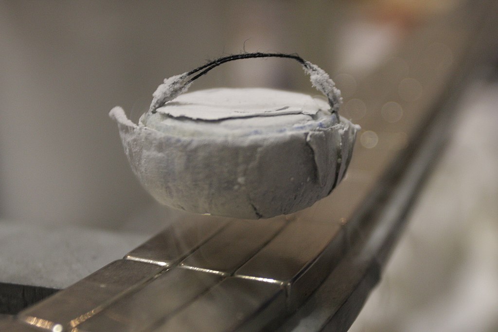
The near-complete expulsion of the magnetic field from a superconducting specimen is called the Meissner effect. In the presence of a magnetic field, the current loops at the periphery will be generated so as to block the entry of the external field inside the specimen. If a magnetic field is allowed within a superconductor, then, by Ampere’s law, there will be normal current within the sample. However, there is no normal current inside the specimen. Thus, there can’t be any magnetic field. For this reason, superconductors are known as perfect diamagnets with very large diamagnetic susceptibility. Even the best-known diamagnets (which are non-superconductors) have magnetic susceptibilities of the order of 10−5. Thus, the diamagnetic property can be considered a distinct property of superconductors compared to zero electrical resistance.
The near-complete expulsion of the magnetic field from a superconducting specimen is called the Meissner effect
A typical experiment demonstrating the Meissner effect can be thought of as follows: Take a superconducting sample (T < Tc), sprinkle iron filings around the sample, and switch on the magnetic field. The iron filings are going to line up in concentric circles around the specimen. This implies the expulsion of the flux lines outside the sample, which makes the filings line up.
Distinction between perfect conductors and superconductors
The distinction between a perfect conductor and a superconductor is brought about by magnetic field-cooled (FC) and zero-field-cooled (ZFc) cases, as shown below in Fig. 1.
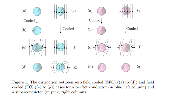
In the absence of an external magnetic field, temperature is lowered for both the metal and the superconductor in their metallic states from T > Tc to T < Tc (see left panel for both in Fig. 1). Hence, a magnetic field is applied, which eventually gets expelled owing to the Meissner effect. The field has finally been withdrawn. However, if cooling is done in the presence of an external field, after the field is withdrawn, the flux lines get trapped for a perfect conductor; however, the superconductor is left with no memory of an applied field, a situation similar to what happens in the zero-field cooling case. So, superconductors have no memory, while perfect conductors have memory.
Microscopic considerations: BCS theory
The first microscopic theory of superconductivity was proposed by Berdeen, Cooper, and Schrieffer (BCS) in 1957, which earned them a Nobel Prize in 1972. The underlying assumption was that an attractive interaction between the electrons is possible, which is mediated via phonons. Thus, electrons form bound pairs under certain conditions, such as (i) two electrons in the vicinity of the filled Fermi Sea within an energy range ¯hωD (set by the phonons or lattice). (ii) The presence of phonons or the underlying lattice is confirmed by the isotope effect experiment, which confirms that the transition temperature is proportional to the mass of ions. Since the Debye frequency depends on the ionic mass, it implies that the lattice must be involved. 3 A small calculation yields that an attractive interaction is possible in a narrow range of energy. This attractive interaction causes the system to be unstable, and a long-range order develops via symmetry breaking. In a book by one of the discoverers, namely, Schrieffer, he described an analogy between a dancing floor comprising couples, dancing one with any other couple, and being completely oblivious to any other couple present in the room. The couples, while dancing, drift from one end of the room to another but do not collide with each other. This implies less dissipation in the transport of a superconductor. The BCS theory explained most of the features of the superconductors known at that time, such as (i) the discontinuity of the specific heat at the transition temperature, Tc. (ii) Involvement of the lattice via the isotope effect. (iii) Estimation of Tc and the energy gap. The value of Tc and the gap are confirmed by tunnelling experiments across metal-superconductor (M-S) or metal-insulator-superconductor (MIS) types of junctions. Giaever was awarded the Nobel Prize in 1973 for his work on these experiments. (iv) The Meissner effect can be explained within a linear response regime. (v) Temperature dependence of the energy gap, confirming gradual vanishing, which confirms a second-order phase transition. Most of the features of conventional superconductors can be explained using BCS theory. Another salient feature of the theory is that it is non-perturbative. There is no small parameter in the problem. The calculations were done with a variational theory where the energy is minimised with respect to some free parameters of the variational wavefunction, known as the BCS wavefunction.
Unconventional Superconductors: High-Tc Cuprates
This is a class of superconductors where the two-dimensional copper oxide planes play the main role, and superconductivity occurs in these planes. Doping these planes with mobile carriers makes the system unstable towards superconducting correlations. At zero doping, the system is an antiferromagnetic insulator (see Fig. 2). With about 15% to 20% doping with foreign elements, such as strontium (Sr), etc. (for example, in La2−xSrxCuO4), the system turns superconductivity. There are two things that are surprising in this regard. (i) The proximity of the insulating state to the superconducting state; (ii) For the system initially in the superconducting state, as the temperature is raised, instead of going into a metallic state, it shows several unfamiliar features that are very unlike the known Fermi liquid characteristics. It is called a strange metal.
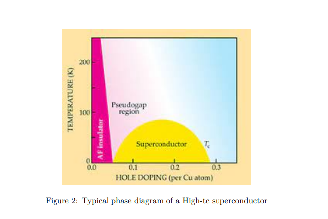
In fact, there are some signatures of pre-formed pairs in the ‘so-called’ metallic state, known as the pseudo gap phase. Since the starting point from which one should build a theory is missing, a complete understanding of the mechanism leading to the phenomenon cannot be understood. It remained a theoretical riddle.
Space & Physics
NASA to launch first crewed Artemis Moon mission on April 1
NASA will launch Artemis II on April 1, marking the first crewed mission around the Moon in over 50 years.

Artemis will be the first human mission to travel beyond low-Earth orbit since the Apollo era, and it is designed as a 10-day journey that will take astronauts on a flyby around the Moon before returning to Earth.
NASA is set to make history with the launch of its first crewed Artemis mission around the Moon, with liftoff targeted for April 1, 2026, marking humanity’s return to deep space exploration after more than five decades.
The mission, known as Artemis II, will carry four astronauts aboard the Orion spacecraft using NASA’s powerful Space Launch System rocket. The launch is scheduled from Kennedy Space Center in Florida, with additional backup launch opportunities extending through early April.
This will be the first human mission to travel beyond low-Earth orbit since the Apollo era, and it is designed as a 10-day journey that will take astronauts on a flyby around the Moon before returning to Earth.
The crew includes NASA astronauts Reid Wiseman, Victor Glover, and Christina Koch, along with Canadian astronaut Jeremy Hansen. The mission is expected to test critical systems such as life support, navigation, and the spacecraft’s heat shield in deep space conditions.
Unlike future Artemis missions, Artemis II will not land on the lunar surface. Instead, it serves as a crucial step toward upcoming missions that aim to establish a sustained human presence on the Moon and eventually enable crewed missions to Mars.
NASA officials say the mission represents a major milestone in space exploration, combining international collaboration and advanced technology to usher in a new era of human spaceflight.
Space & Physics
Magnetic Fields Found to Shape Star Formation Near Milky Way Disc
Scientists map magnetic fields in molecular clouds near the Milky Way, revealing their key role in slowing and shaping star formation.

Scientists map magnetic fields in molecular clouds near the Milky Way, revealing their key role in slowing and shaping star formation.
Scientists have uncovered new insights into how stars are formed by mapping the magnetic fields surrounding molecular clouds near the Milky Way’s disc, offering a deeper understanding of one of the universe’s most fundamental processes.
The study focuses on two small molecular clouds—L1604 and L121—revealing how magnetic fields influence the balance between gravity and internal pressure during star formation.
Magnetic Fields Star Formation in Milky Way Clouds
For decades, astronomers have understood star formation as a balance between gravity pulling gas inward and internal pressure pushing outward. However, the new research highlights a third critical factor: magnetic fields.
In a media statement, the researchers explained that magnetic fields act as an invisible force shaping how molecular clouds evolve and collapse to form stars.
The study was conducted by scientists from the Aryabhatta Research Institute of Observational Sciences (ARIES)m Uttarakhand, India and Assam University, using advanced polarimetric techniques to detect otherwise invisible magnetic structures.
Magnetic Fields Star Formation Observed Using Polarimetry
To map these fields, the team used R-band polarimetry with the ARIES Imaging Polarimeter mounted on a 104-cm telescope in Nainital.
This technique measures how starlight becomes polarised as it passes through dust grains aligned by magnetic fields.
In a media statement, the researchers said that by analysing thousands of such light signals, they were able to “see” the skeleton of magnetic fields surrounding the molecular clouds for the first time.
Two Molecular Clouds Reveal Contrasting Behaviour
The study examined two distinct clouds:
- L1604, located about 816 parsecs away, is dense and massive, with strong potential for future star formation
- L121, much closer at 124 parsecs, is less dense but exhibits a stronger and more organised magnetic field
In a media statement, the scientists noted that the orderly magnetic structure in L121 suggests it has not yet undergone intense gravitational collapse, unlike more active star-forming regions.
Magnetic Fields Star Formation Controlled by Energy Balance
By calculating magnetic field strength, the researchers found that both clouds are sub-critical, meaning magnetic forces are strong enough to resist gravitational collapse across most of their structure.
In a media statement, the team stated that magnetic energy dominates over both turbulence and gravity at the outer regions of the clouds.
However, deep within the dense cores, gravity may begin to take over, creating conditions suitable for star formation.
The “Recipe” for Star Formation
The findings suggest that magnetic fields play a crucial role in regulating how quickly stars form.
In a media statement, researchers said that magnetism acts as an “invisible hand,” slowing down star formation and preventing galaxies from converting all their gas into stars at once.
The study positions L1604 and L121 as natural laboratories for understanding the interplay between gravity and magnetism.
Rather than being passive clouds, they represent dynamic systems where fundamental forces interact over millions of years to shape the birth of stars.
The findings offer a clearer picture of how galaxies like the Milky Way sustain star formation over long cosmic timescales, balancing collapse with control.
Space & Physics
Researchers Use AI to Enable Robots to ‘See’ Through Walls
MIT researchers develop AI-powered system using wireless signals to help robots see through walls and reconstruct hidden objects and indoor spaces.
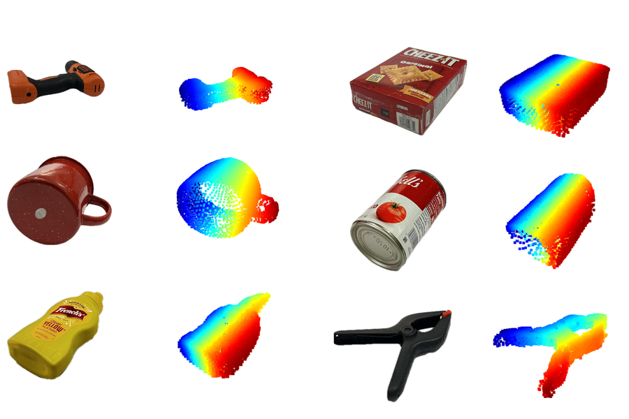
Researchers at Massachusetts Institute of Technology have developed a new artificial intelligence-powered system that allows robots to detect and reconstruct objects hidden behind walls and obstacles, marking a significant breakthrough in machine perception.
The system combines wireless signals with generative AI models to enable what researchers describe as a new form of “wireless vision,” potentially transforming robotics, logistics, and smart environments.
AI See Through Walls Using Wireless Signals
The research builds on over a decade of work using millimeter wave (mmWave) signals—similar to those used in Wi-Fi—which can pass through materials such as drywall, plastic, and cardboard and reflect off hidden objects.
Earlier approaches could only capture partial shapes due to limitations in how these signals reflect.
The new system overcomes this by combining wireless reflections with generative AI, enabling the reconstruction of complete object shapes even when they are not directly visible.
“What we’ve done now is develop generative AI models that help us understand wireless reflections. This opens up a lot of interesting new applications, but technically it is also a qualitative leap in capabilities, from being able to fill in gaps we were not able to see before to being able to interpret reflections and reconstruct entire scenes,” said Fadel Adib, in a media statement.
“We are using AI to finally unlock wireless vision.”
AI See Through Walls Improves Object Reconstruction
The system, called Wave-Former, first creates a partial image of a hidden object using reflected wireless signals. It then uses a trained AI model to fill in missing parts and refine the reconstruction.
In tests, Wave-Former successfully reconstructed around 70 everyday objects—including boxes, utensils, and fruits—with nearly 20% higher accuracy than existing methods.
The objects were placed behind or under materials such as wood, fabric, and plastic, demonstrating the system’s robustness in real-world conditions.
AI See Through Walls Reconstructs Entire Rooms
Beyond individual objects, the researchers developed a second system capable of reconstructing entire indoor environments.
Using a single stationary radar, the system tracks how wireless signals bounce off moving humans and surrounding objects. These reflections—often considered noise—are analysed by AI to map out the room layout.
The system, known as RISE, was tested using over 100 human movement patterns and achieved twice the accuracy of existing techniques in reconstructing indoor spaces.
Privacy-Preserving Alternative to Cameras
Unlike camera-based systems, this approach does not capture visual images, offering a privacy-preserving alternative for indoor monitoring and robotics.
Because it relies on wireless signals rather than cameras, it can detect presence and layout without revealing identifiable details.
Applications in Warehousing and Smart Homes
The researchers say the technology could have wide-ranging applications:
- Warehouses: Robots could verify packed items before shipping, reducing errors and returns
- Smart homes: Robots could better understand human location and movement
- Human-robot interaction: Improved safety and efficiency in shared environments
The system could also pave the way for future “foundation models” trained specifically on wireless data, similar to how large AI models are trained for language and vision.
-

 Society3 months ago
The Ten-Rupee Doctor Who Sparked a Health Revolution in Kerala’s Tribal Highlands
-

 Society3 months ago
From Qubits to Folk Puppetry: India’s Biggest Quantum Science Communication Conclave Wraps Up in Ahmedabad
-

 COP305 months ago
Brazil Cuts Emissions by 17% in 2024—Biggest Drop in 16 Years, Yet Paris Target Out of Reach
-

 Women In Science6 months ago
The Data Don’t Lie: Women Are Still Missing from Science — But Why?
-

 Earth5 months ago
Data Becomes the New Oil: IEA Says AI Boom Driving Global Power Demand
-

 COP305 months ago
Corporate Capture: Fossil Fuel Lobbyists at COP30 Hit Record High, Outnumbering Delegates from Climate-Vulnerable Nations
-

 Space & Physics4 months ago
Indian Physicists Win 2025 ICTP Prize for Breakthroughs in Quantum Many-Body Physics
-

 Health5 months ago
Air Pollution Claimed 1.7 Million Indian Lives and 9.5% of GDP, Finds The Lancet


